Character lcd interface signals, Voltage compatibility, Interaction with intel strataflash – Digilent 410-087P-KIT User Manual
Page 42
42
Spartan-3E Starter Kit Board User Guide
UG230 (v1.0) March 9, 2006
Chapter 5: Character LCD Screen
R
Character LCD Interface Signals
shows the interface character LCD interface signals.
Voltage Compatibility
The character LCD is power by +5V. The FPGA I/O signals are powered by 3.3V.
However, the FPGA’s output levels are recognized as valid Low or High logic levels by the
LCD. The LCD controller accepts 5V TTL signal levels and the 3.3V LVCMOS outputs
provided by the FPGA meet the 5V TTL voltage level requirements.
The 390
Ω series resistors on the data lines prevent overstressing on the FPGA and
StrataFlash I/O pins when the character LCD drives a High logic value. The character LCD
drives the data lines when LCD_RW is High. Most applications treat the LCD as a write-
only peripheral and never read from from the display.
Interaction with Intel StrataFlash
As shown in
, the four LCD data signals are also shared with StrataFlash data
lines SF_D<11:8>. As shown in
, the LCD/StrataFlash interaction depends on the
application usage in the design. When the StrataFlash memory is disabled (SF_CE0 =
High), then the FPGA application has full read/write access to the LCD. Conversely, when
LCD read operations are disabled (LCD_RW = Low), then the FPGA application has full
read/write access to the StrataFlash memory
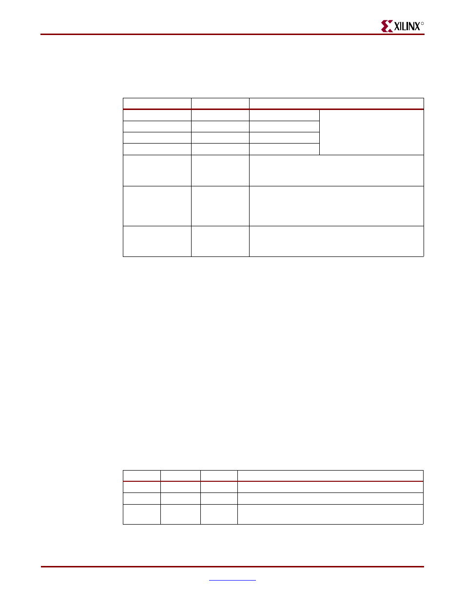
Table 5-1:
Character LCD Interface
Signal Name
FPGA Pin
Function
SF_D<11>
M15
Data bit DB7
Shared with StrataFlash pins
SF_D<11:8>
SF_D<10>
P17
Data bit DB6
SF_D<9>
R16
Data bit DB5
SF_D<8>
R15
Data bit DB4
LCD_E
M18
Read/Write Enable Pulse
0: Disabled
1: Read/Write operation enabled
LCD_RS
L18
Register Select
0: Instruction register during write operations. Busy
Flash during read operations
1: Data for read or write operations
LCD_RW
L17
Read/Write Control
0: WRITE, LCD accepts data
1: READ, LCD presents data
Table 5-2:
LCD/StrataFlash Control Interaction
SF_CE0
SF_BYTE
LCD_RW
Operation
1
X
X
StrataFlash disabled. Full read/write access to LCD.
X
X
0
LCD write access only. Full access to StrataFlash.
X
0
X
StrataFlash in byte-wide (x8) mode.
Upper data lines
are not used. Full access to both LCD and StrataFlash.
Notes:
1. ‘X’ indicates a don’t care, can be either 0 or 1.