Spi communication details, Communication protocol, Spi communication details communication protocol – Digilent 410-087P-KIT User Manual
Page 69: Table 9-2
Spartan-3E Starter Kit Board User Guide
69
UG230 (v1.0) March 9, 2006
SPI Communication
R
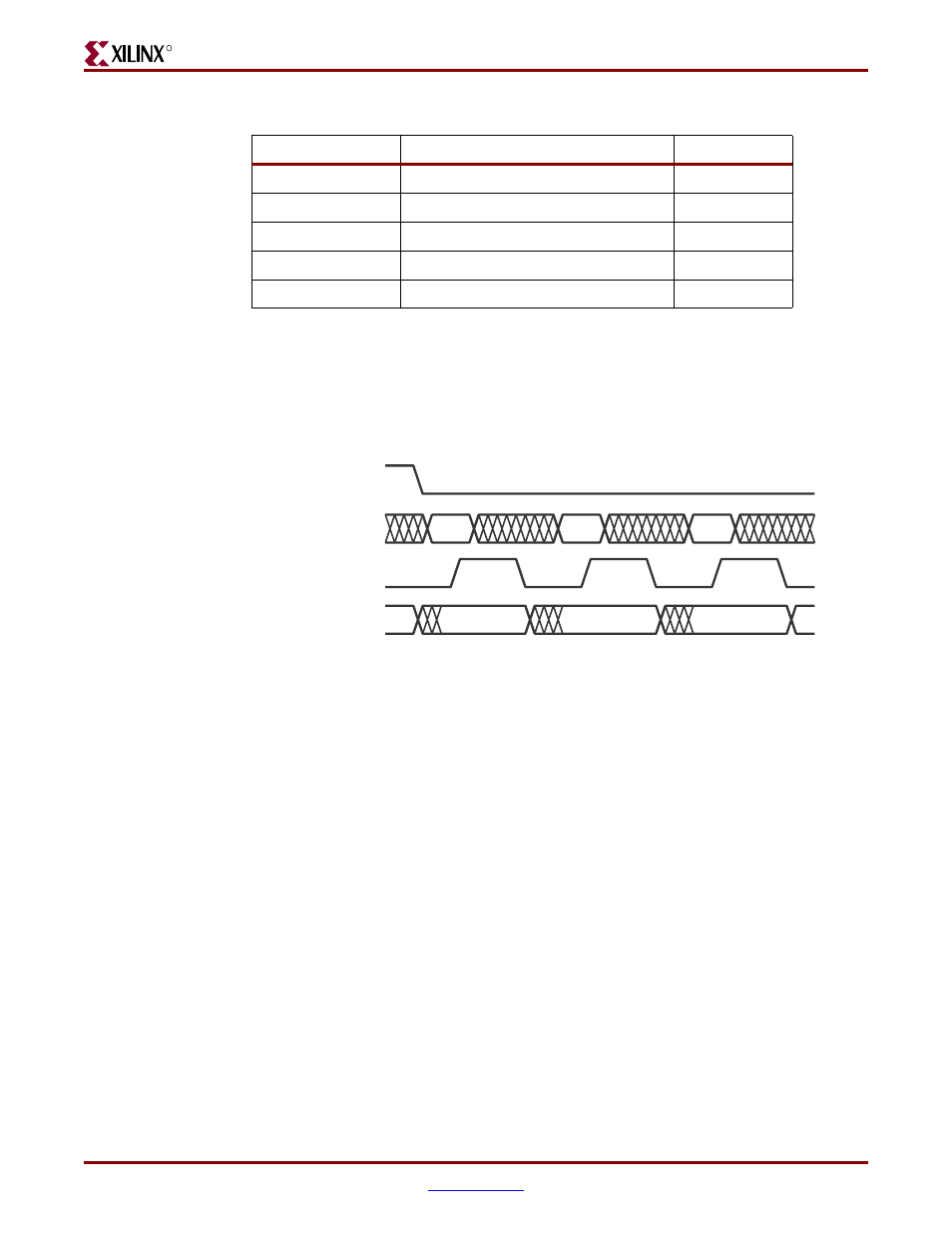
SPI Communication Details
shows a detailed example of the SPI bus timing. Each bit is transmitted or
received relative to the SPI_SCK clock signal. The bus is fully static and supports clocks
rate up to the maximum of 50 MHz. However, check all timing parameters using the
LTC2624 data sheet if operating at or close to the maximum speed.
After driving the DAC_CS slave select signal Low, the FPGA transmits data on the
SPI_MOSI signal, MSB first. The LTC2624 captures input data (SPI_MOSI) on the rising
edge of SPI_SCK; the data must be valid for at least 4 ns relative to the rising clock edge.
The LTC2624 DAC transmits its data on the SPI_MISO signal on the falling edge of
SPI_SCK. The FPGA captures this data on the next rising SPI_SCK edge. The FPGA must
read the first SPI_MISO value on the first rising SPI_SCK edge after DAC_CS goes Low.
Otherwise, bit 31 is missed.
After transmitting all 32 data bits, the FPGA completes the SPI bus transaction by
returning the DAC_CS slave select signal High. The High-going edge starts the actual
digital-to-analog conversion process within the DAC.
Communication Protocol
shows the communications protocol required to interface with the LTC2624
DAC. The DAC supports both a 24-bit and 32-bit protocol. The 32-bit protocol is shown.
Inside the D/A converter, the SPI interface is formed by a 32-bit shift register. Each 32-bit
command word consists of a command, an address, followed by data value. As a new
command enters the DAC, the previous 32-bit command word is echoed back to the
master. The response from the DAC can be ignored although it is a useful to confirm
correct communication.
Table 9-2:
Disabled Devices on the SPI Bus
Signal
Disabled Device
Disable Value
SPI_SS_B
SPI serial Flash
1
AMP_CS
Programmable pre-amplifier
1
AD_CONV
Analog-to-Digital Converter (ADC)
0
SF_CE0
StrataFlash Parallel Flash PROM
1
FPGA_INIT_B
Platform Flash PROM
1
Figure 9-3:
SPI Communication Waveforms
DAC_CS
SPI_MOSI
SPI_SCK
SPI_MISO
Previous 31
31
30
29
Previous 30
Previous 29
UG230_c9_03_021806