Interface signals, Figure 9-2 – Digilent 410-087P-KIT User Manual
Page 68
68
Spartan-3E Starter Kit Board User Guide
UG230 (v1.0) March 9, 2006
Chapter 9: Digital to Analog Converter (DAC)
R
Interface Signals
lists the interface signals between the FPGA and the DAC. The SPI_MOSI,
SPI_MISO, and SPI_SCK signals are shared with other devices on the SPI bus. The
DAC_CS signal is the active-Low slave select input to the DAC. The DAC_CLR signal is
the active-Low, asynchronous reset input to the DAC.
The serial data output from the DAC is primarily used to cascade multiple DACs. This
signal can be ignored in most applications although it does demonstrate full-duplex
communication over the SPI bus.
Disable Other Devices on the SPI Bus to Avoid Contention
The SPI bus signals are shared by other devices on the board. It is vital that other devices
are disabled when the FPGA communicates with the DAC to avoid bus contention.
provides the signals and logic values required to disable the other devices.
Although the StrataFlash PROM is a parallel device, its least-significant data bit is shared
with the SPI_MISO signal.
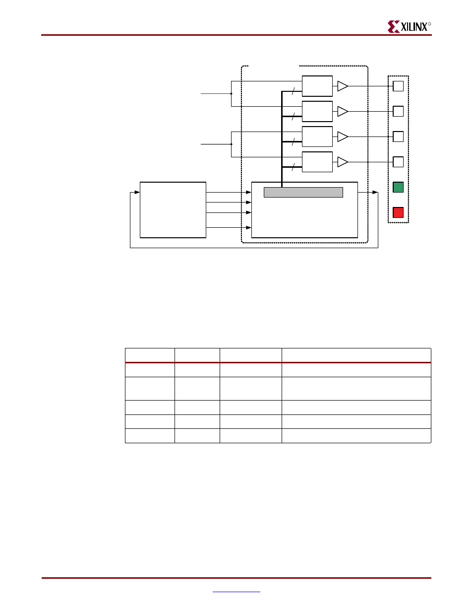
Figure 9-2:
Digital-to-Analog Connection Schematics
Header J5
DAC A
12
DAC B
12
DAC C
12
12
SPI_MOSI
DAC_CS
SPI_SCK
DAC_CLR
CS/LD
SDI
SCK
CLR
SDO
SPI_MISO
(N10)
(T4)
(U16)
(P8)
(N8)
3.3V
2.5V
A
B
C
D
GND
VCC
REF A
REF B
REF C
REF D
VOUTA
VOUTB
VOUTC
VOUTD
Spartan-3E FPGA
DAC D
LTC 2624 DAC
SPI Control Interface
(3.3V)
UG230_c9_02_021806
Table 9-1:
DAC Interface Signals
Signal
FPGA Pin
Direction
Description
SPI_MOSI
T4
FPGAÆDAC
Serial data: Master Output, Slave Input
DAC_CS
N8
FPGAÆDAC
Active-Low chip-select. Digital-to-analog
conversion starts when signal returns High.
SPI_SCK
U16
FPGAÆDAC
Clock
DAC_CLR
P8
FPGAÆDAC
Asynchronous, active-Low reset input
SPI_MISO
N10
FPGAÅDAC
Serial data: Master Input, Slave Output