Clock connections, Voltage control, 50 mhz on-board oscillator – Digilent 410-087P-KIT User Manual
Page 22: Auxiliary clock oscillator socket, Sma clock input or output connector, Ucf constraints, Location
22
Spartan-3E Starter Kit Board User Guide
UG230 (v1.0) March 9, 2006
Chapter 3: Clock Sources
R
Clock Connections
Each of the clock inputs connect directly to a global buffer input in I/O Bank 0, along the
top of the FPGA. As shown in
, each of the clock inputs also optimally connects to
an associated DCM.
Voltage Control
The voltage for all I/O pins in FPGA I/O Bank 0 is controlled by jumper JP9.
Consequently, these clock resources are also controlled by jumper JP9. By default, JP9 is set
for 3.3V. The on-board oscillator is a 3.3V device and might not perform as expected when
jumper JP9 is set for 2.5V.
50 MHz On-Board Oscillator
The board includes a 50 MHz oscillator with a 40% to 60% output duty cycle. The oscillator
is accurate to
±
2500 Hz or
±
50 ppm.
Auxiliary Clock Oscillator Socket
The provided 8-pin socket accepts clock oscillators that fit the 8-pin DIP footprint. Use this
socket if the FPGA application requires a frequency other than 50 MHz. Alternatively, use
the FPGA’s Digital Clock Manager (DCM) to generate or synthesize other frequencies from
the on-board 50 MHz oscillator.
SMA Clock Input or Output Connector
To provide a clock from an external source, connect the input clock signal to the SMA
connector. The FPGA can also generate a single-ended clock output or other high-speed
signal on the SMA clock connector for an external device.
UCF Constraints
The clock input sources require two different types of constraints. The location constraints
define the I/O pin assignments and I/O standards. The period constraints define the clock
period—and consequently the clock frequency—and the duty cycle of the incoming clock
signal.
Location
provides the UCF constraints for the three clock input sources, including the
I/O pin assignment and the I/O standard used. The settings assume that jumper JP9 is set
for 3.3V. If JP9 is set for 2.5V, adjust the IOSTANDARD settings accordingly.
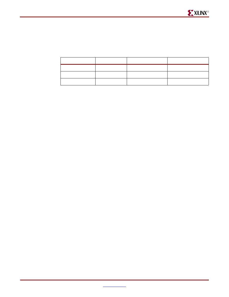
Table 3-1:
Clock Inputs and Associated Global Buffers and DCMs
Clock Input
FPGA Pin
Global Buffer
Associated DCM
CLK_50MHZ
C9
GCLK10
DCM_X0Y1
CLK_AUX
B8
GCLK8
DCM_X0Y1
CLK_SMA
A10
GCLK7
DCM_X1Y1