Atmega16(l) – Rainbow Electronics ATmega64L User Manual
Page 59
59
ATmega16(L)
2466B–09/01
an open drain driver with slew-rate limitation. When this pin is used by the 2-wire Serial
Interface, the pull-up can still be controlled by the PORTC1 bit.
• SCL - Port C, Bit 0
SCL, 2-wire Serial Interface Clock: When the TWEN bit in TWCR is set (one) to enable
the 2-wire Serial Interface, pin PC0 is disconnected from the port and becomes the
Serial Clock I/O pin for the 2-wire Serial Interface. In this mode, there is a spike filter on
the pin to suppress spikes shorter than 50 ns on the input signal, and the pin is driven by
an open drain driver with slew-rate limitation. When this pin is used by the 2-wire Serial
Interface, the pull-up can still be controlled by the PORTC0 bit.
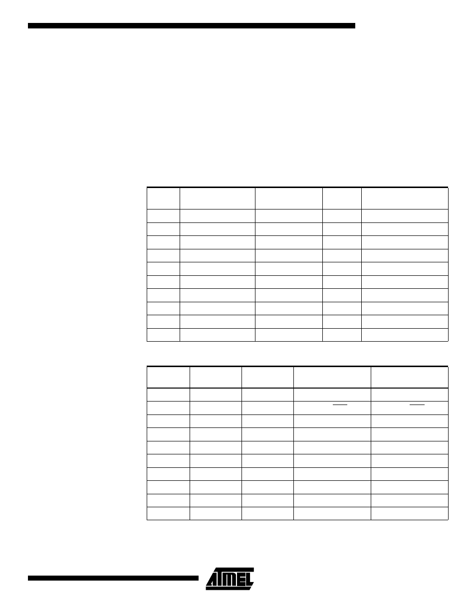
Table 29 and Table 30 relate the alternate functions of Port C to the overriding signals
shown in Figure 26 on page 52.
Note:
1. When enabled, the Two-Wire Serial Interface enables slew-rate controls on the output
pins PC0 and PC1. This is not shown in the figure. In addition, spike filters are con-
nected between the AIO outputs shown in the port figure and the digital logic of the
TWI module.
Table 29. Overriding Signals for Alternate Functions in PC7..PC4
Signal
Name
PC7/TOSC2
PC6/TOSC1
PC5/TDI
PC4/TDO
PUOE
AS2
AS2
JTAGEN
JTAGEN
PUOV
0
0
1
0
DDOE
AS2
AS2
JTAGEN
JTAGEN
DDOV
0
0
0
SHIFT_IR + SHIFT_DR
PVOE
0
0
0
JTAGEN
PVOV
0
0
0
TDO
DIEOE
AS2
AS2
JTAGEN
JTAGEN
DIEOV
0
0
0
0
DI
–
–
–
–
AIO
T/C2 OSC OUTPUT
T/C2 OSC INPUT
TDI
–
Table 30. Overriding Signals for Alternate Functions in PC3..PC0
Signal
Name
PC3/TMS
PC2/TCK
PC1/SDA
PC0/SCL
PUOE
JTAGEN
JTAGEN
TWEN
TWEN
PUOV
1
1
PORTC1 • PUD
PORTC0 • PUD
DDOE
JTAGEN
JTAGEN
TWEN
TWEN
DDOV
0
0
SDA_OUT
SCL_OUT
PVOE
0
0
TWEN
TWEN
PVOV
0
0
0
0
DIEOE
JTAGEN
JTAGEN
0
0
DIEOV
0
0
0
0
DI
–
–
–
–
AIO
TMS
TCK
SDA INPUT
SCL INPUT