Output compare unit, Atmega16(l) – Rainbow Electronics ATmega64L User Manual
Page 113
113
ATmega16(L)
2466B–09/01
top
Signalizes that TCNT2 has reached maximum value.
bottom
Signalizes that TCNT2 has reached minimum value (zero).
Depending on the mode of operation used, the counter is cleared, incremented, or dec-
remented at each timer clock (clk
T2
). clk
T2
can be generated from an external or internal
clock source, selected by the clock select bits (CS22:0). When no clock source is
selected (CS22:0 = 0) the timer is stopped. However, the TCNT2 value can be accessed
by the CPU, regardless of whether clk
T2
is present or not. A CPU write overrides (has
priority over) all counter clear or count operations.
The counting sequence is determined by the setting of the WGM21 and WGM20 bits
located in the Timer/Counter control register (TCCR2). There are close connections
between how the counter behaves (counts) and how waveforms are generated on the
output compare output OC2. For more details about advanced counting sequences and
waveform generation, see “Modes of Operation” on page 115.
The Timer/Counter overflow (TOV2) flag is set according to the mode of operation
selected by the WGM21:0 bits.
TOV2
can be used for generating a CPU interrupt.
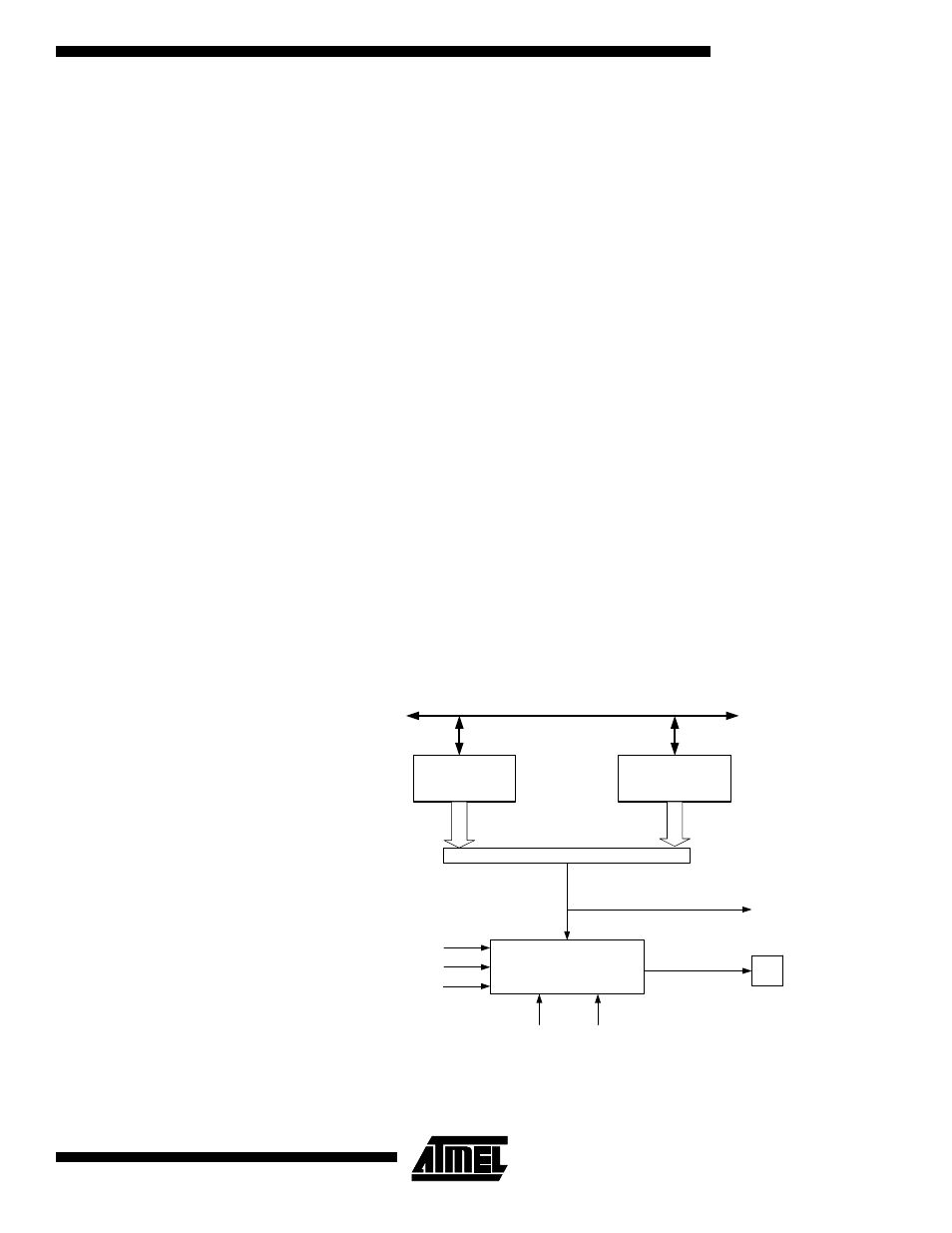
Output Compare Unit
The 8-bit comparator continuously compares TCNT2 with the output compare register
(OCR2). Whenever TCNT2 equals OCR2, the comparator signals a match. A match will
set the output compare flag (OCF2) at the next timer clock cycle. If enabled (OCIE2 = 1),
the output compare flag generates an output compare interrupt. The OCF2 flag is auto-
matically cleared when the interrupt is executed. Alternatively, the OCF2 flag can be
cleared by software by writing a logical one to its I/O bit location. The waveform genera-
tor uses the match signal to generate an output according to operating mode set by the
WGM21:0 bits and compare output mode (COM21:0) bits. The max and bottom signals
are used by the waveform generator for handling the special cases of the extreme val-
ues in some modes of operation (“Modes of Operation” on page 115). Figure 55 shows
a block diagram of the output compare unit.
Figure 55. Output Compare Unit, Block Diagram
The OCR2 register is double buffered when using any of the pulse width modulation
(PWM) modes. For the normal and clear timer on compare (CTC) modes of operation,
the double buffering is disabled. The double buffering synchronizes the update of the
OCFn (Int.Req.)
=
(8-bit Comparator )
OCRn
OCxy
DATA BUS
TCNTn
WGMn1:0
Waveform Generator
top
FOCn
COMn1:0
bottom