Spi status register – spsr, Atmega16(l) – Rainbow Electronics ATmega64L User Manual
Page 133
133
ATmega16(L)
2466B–09/01
• Bit 3 - CPOL: Clock Polarity
When this bit is written to one, SCK is high when idle. When CPOL is written to zero,
SCK is low when idle. Refer to Figure 67 and Figure 68 for an example. The CPOL func-
tionality is summarized below:
• Bit 2 - CPHA: Clock Phase
The settings of the clock phase bit (CPHA) determine if data is sampled on the leading
(first) or trailing (last) edge of SCK. Refer to Figure 67 and Figure 68 for an example.
The CPOL functionality is summarized below:
• Bits 1,0 - SPR1, SPR0: SPI Clock Rate Select 1 and 0
These two bits control the SCK rate of the device configured as a master. SPR1 and
SPR0 have no effect on the slave. The relationship between SCK and the Oscillator
Clock frequency f
osc
is shown in the following table:
SPI Status Register – SPSR
• Bit 7 - SPIF: SPI Interrupt Flag
When a serial transfer is complete, the SPIF flag is set. An interrupt is generated if SPIE
in SPCR is set and global interrupts are enabled. If SS is an input and is driven low
when the SPI is in master mode, this will also set the SPIF flag. SPIF is cleared by hard-
ware when executing the corresponding interrupt handling vector. Alternatively, the
Table 56. CPOL Functionality
CPOL
Leading Edge
Trailing Edge
0
Rising
Falling
1
Falling
Rising
Table 57. CPHA Functionality
CPHA
Leading Edge
Trailing Edge
0
Sample
Setup
1
Setup
Sample
Table 58. Relationship Between SCK and the Oscillator Frequency
SPI2X
SPR1
SPR0
SCK Frequency
0
0
0
f
osc
/
4
0
0
1
f
osc
/
16
0
1
0
f
osc
/
64
0
1
1
f
osc
/
128
1
0
0
f
osc
/
2
1
0
1
f
osc
/
8
1
1
0
f
osc
/
32
1
1
1
f
osc
/
64
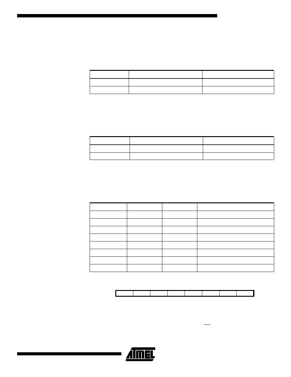
Bit
7
6
5
4
3
2
1
0
SPIF
WCOL
–
–
–
–
–
SPI2X
SPSR
Read/Write
R
R
R
R
R
R
R
R/W
Initial Value
0
0
0
0
0
0
0
0