Atmega16(l) – Rainbow Electronics ATmega64L User Manual
Page 50
50
ATmega16(L)
2466B–09/01
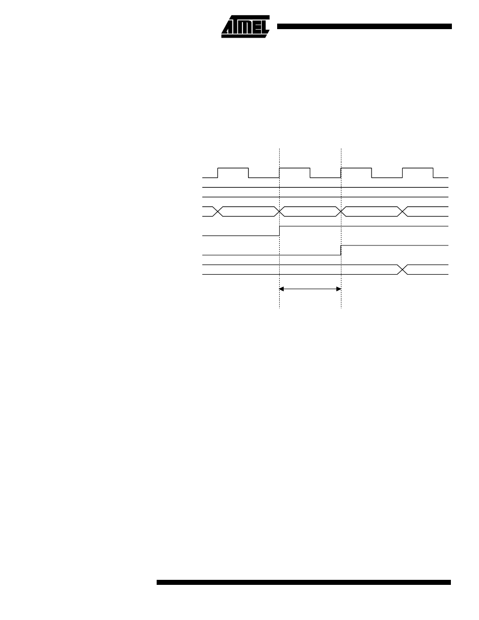
ceeding positive clock edge. As indicated by the two arrows t
pd,max
and t
pd,min
, a single
signal transition on the pin will be delayed between ½ and 1-½ system clock period
depending upon the time of assertion.
When reading back a software assigned pin value, a nop instruction must be inserted as
indicated in Figure 25. The out instruction sets the “SYNC LATCH” signal at the positive
edge of the clock. In this case, the delay t
pd
through the synchronizer is 1 system clock
period.
Figure 25. Synchronization when Reading a Software Assigned Pin Value
The following code example shows how to set port B pins 0 and 1 high, 2 and 3 low, and
define the port pins from 4 to 7 as input with pull-ups assigned to port pins 6 and 7. The
resulting pin values are read back again, but as previously discussed, a nop instruction
is included to be able to read back the value recently assigned to some of the pins.
nop
in r17, PINx
0xFF
0x00
0xFF
t
pd
out PORTx, r16
SYSTEM CLK
r16
INSTRUCTIONS
SYNC LATCH
PINxn
r17