Figure 124 s, Atmega16(l) – Rainbow Electronics ATmega64L User Manual
Page 233
233
ATmega16(L)
2466B–09/01
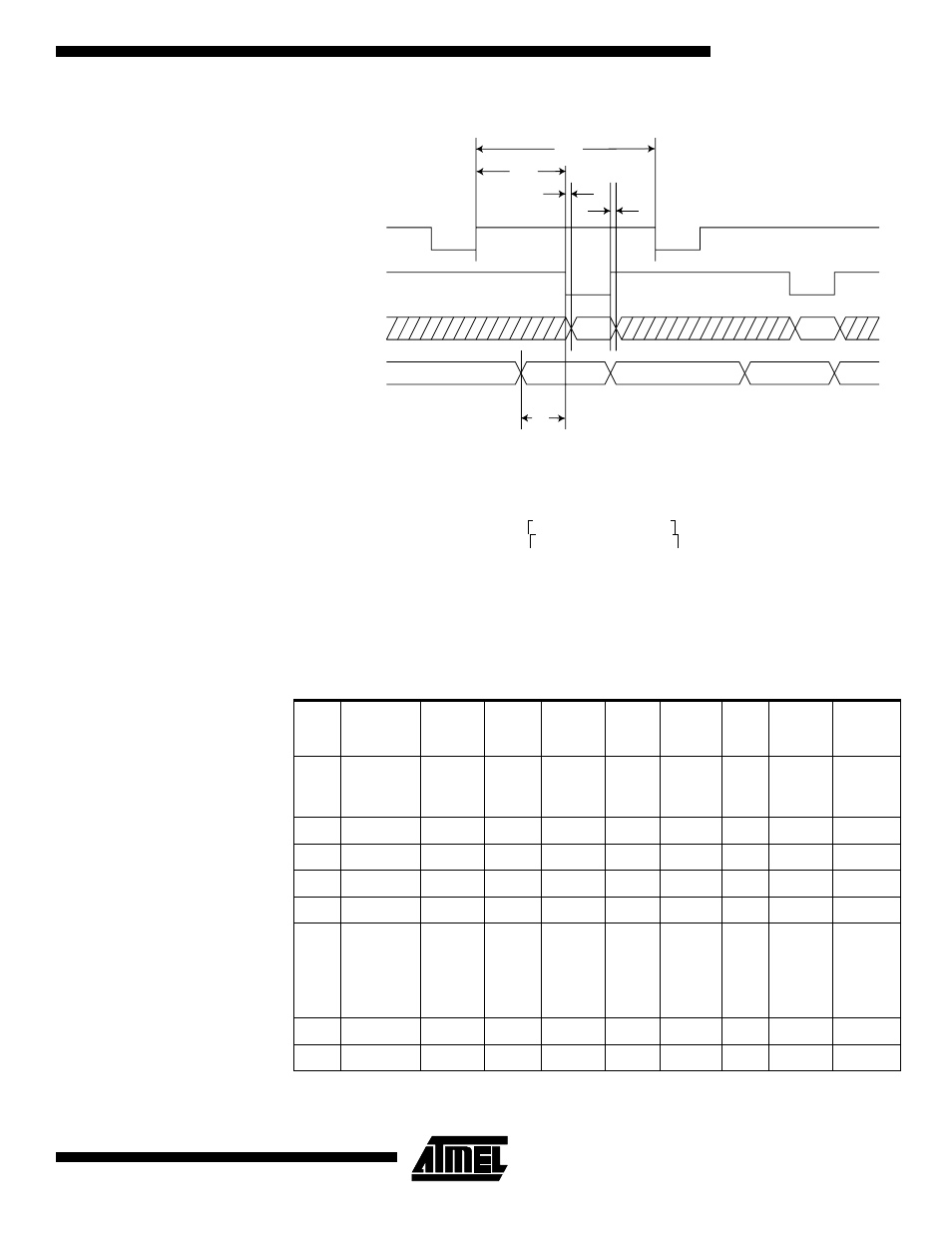
Figure 124. ADC Timing Diagram and Timing Constraints
As an example, consider the task of verifying a 1.5V ± 5% input signal at ADC channel 3
when the power supply is 5.0V and AREF is externally connected to V
CC
.
The recommended values from Table 91 are used unless other values are given in the
algorithm in Table 93. Only the DAC and Port Pin values of the Scan-Chain are shown.
The column “Actions” describes what JTAG instruction to be used before filling the
Boundary-scan register with the succeeding columns. The verification should be done
on the data scanned out when scanning in the data on the same row in the table.
Table 93. Algorithm for Using the ADC
Step
Actions
ADCEN
DAC
MUXEN
HOLD
PRECH
PA3.
Data
PA3.
Control
PA3.
Pullup_
Enable
1
SAMPLE
_PRELO
AD
1
0x200
0x08
1
1
0
0
0
2
EXTEST
1
0x200
0x08
0
1
0
0
0
3
1
0x200
0x08
1
1
0
0
0
4
1
0x123
0x08
1
1
0
0
0
5
1
0x123
0x08
1
0
0
0
0
6
Verify the
COMP bit
scanned
out to be
0
1
0x200
0x08
1
1
0
0
0
7
1
0x200
0x08
0
1
0
0
0
8
1
0x200
0x08
1
1
0
0
0
t
s
t
t
t
h
hold
hp
HOLD
PRECH
COMP
DAC
0x200
0x200
0x
t
d
The lower limit is: 1024 1.5V 0,95 5V
⁄
⋅
⋅
291
0x123
=
=
The upper limit is: 1024 1.5V 1.05 5V
⁄
⋅
⋅
323
0x143
=
=