Serial programming pin mapping, Serial programming algorithm, Atmega16(l) – Rainbow Electronics ATmega64L User Manual
Page 266
266
ATmega16(L)
2466B–09/01
Serial Programming Pin
Mapping
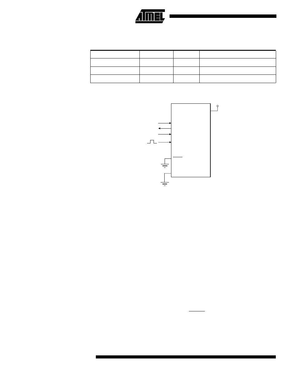
Figure 136. Serial Programming and Verify
Note:
If the device is clocked by the internal oscillator, it is no need to connect a clock source to
the XTAL1 pin.
When programming the EEPROM, an auto-erase cycle is built into the self-timed pro-
gramming operation (in the serial mode ONLY) and there is no need to first execute the
Chip Erase instruction. The Chip Erase operation turns the content of every memory
location in both the Program and EEPROM arrays into $FF.
Depending on CKSEL Fuses, a valid clock must be present. The minimum low and high
periods for the serial clock (SCK) input are defined as follows:
Low:> 2 CPU clock cycles for f
ck
< 12 MHz, 3 CPU clock cycles for f
ck
≥ 12 MHz
High:> 2 CPU clock cycles for f
ck
< 12 MHz, 3 CPU clock cycles for f
ck
≥ 12 MHz
Serial Programming
Algorithm
When writing serial data to the ATmega16, data is clocked on the rising edge of SCK.
When reading data from the ATmega16, data is clocked on the falling edge of SCK. See
Figure 137, Figure 138 and Table 117 for timing details.
To program and verify the ATmega16 in the serial programming mode, the following
sequence is recommended (See four byte instruction formats in Table 116
1.
Power-up sequence:
Apply power between V
CC
and GND while RESET and SCK are set to "0". In
some systems, the programmer can not guarantee that SCK is held low during
Table 114. Pin Mapping Serial Programming
Symbol
Pins
I/O
Description
MOSI
PB5
I
Serial data in
MISO
PB6
O
Serial data out
SCK
PB7
I
Serial clock
VCC
GND
XTAL1
SCK
MISO
MOSI
RESET
PB5
PB6
PB7
+2.7 - 5.5V