Boundary-scan and the two- wire interface, Figure 117, Figure 117 t – Rainbow Electronics ATmega64L User Manual
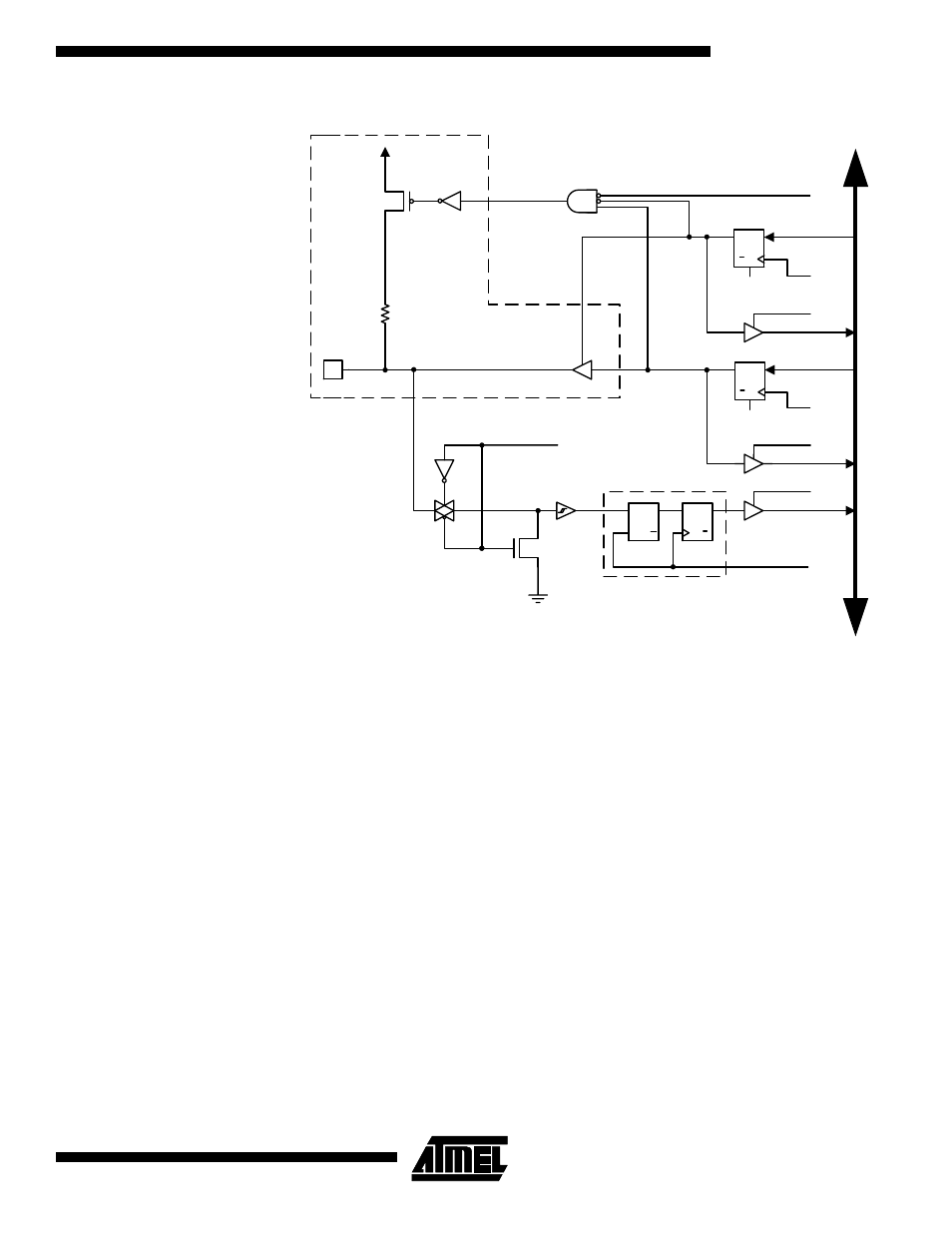
Page 225: Atmega16(l), Figure 117. general port pin schematic diagram, Data b u s
225
ATmega16(L)
2466B–09/01
Figure 117. General Port Pin Schematic Diagram
Note:
1. See Boundary-scan descriptin for details.
Boundary-scan and the Two-
wire Interface
The 2 Two-Wire Interface pins SCL and SDA have one additional control signal in the
scan-chain; Two-Wire Interface Enable – TWIEN. As shown in Figure 118, the TWIEN
signal enables a tri-state buffer with slew-rate control in parallel with the ordinary digital
port pins. A general scan cell as shown in Figure 122 is attached to the TWIEN signal.
Notes:
1. A separate scan chain for the 50 ns spike filter on the input is not provided. The ordi-
nary scan support for digital port pins suffice for connectivity tests. The only reason
for having TWIEN in the scan path, is to be able to disconnect the slew-rate control
buffer when doing boundary-scan.
2. Make sure the OC and TWIEN signals are not asserted simultaneously, as this will
lead to drive contention.
CLK
RPx
RRx
WPx
RDx
WDx
PUD
SYNCHRONIZER
WDx:
WRITE DDRx
WPx:
WRITE PORTx
RRx:
READ PORTx REGISTER
RPx:
READ PORTx PIN
PUD:
PULLUP DISABLE
CLK :
I/O CLOCK
RDx:
READ DDRx
D
L
Q
Q
RESET
RESET
Q
Q
D
Q
Q
D
CLR
PORTxn
Q
Q
D
CLR
DDxn
PINxn
D
ATA
B
U
S
SLEEP
SLEEP:
SLEEP CONTROL
Pxn
I/O
I/O
PUExn
OCxn
ODxn
IDxn
PUExn:
PULLUP ENABLE for pin Pxn
OCxn:
OUTPUT CONTROL for pin Pxn
ODxn:
OUTPUT DATA to pin Pxn
IDxn:
INPUT DATA from pin Pxn