Offset compensation schemes, Adc accuracy definitions, Atmega16(l) – Rainbow Electronics ATmega64L User Manual
Page 205
205
ATmega16(L)
2466B–09/01
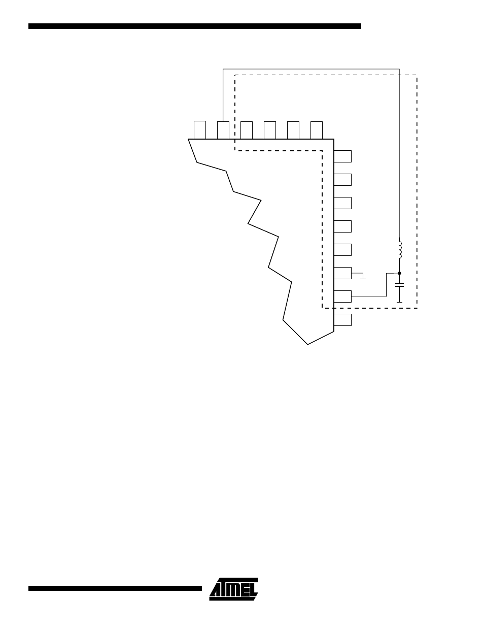
Figure 106. ADC Power Connections
Offset Compensation
Schemes
The gain stage has a built-in offset cancellation circuitry that nulls the offset of differen-
tial measurements as much as possible. The remaining offset in the analog path can be
measured directly by selecting the same channel for both differential inputs. This offset
residue can be then subtracted in software from the measurement results. Using this
kind of software based offset correction, offset on any channel can be reduced below
one LSB.
ADC Accuracy Definitions
An n-bit single-ended ADC converts a voltage linearly between GND and V
REF
in 2
n
steps (LSBs). The lowest code is read as 0, and the highest code is read as 2
n
-1.
Several parameters describe the deviation from the ideal behavior:
•
Offset: The deviation of the first transition (0x000 to 0x001) compared to the ideal
transition (at 0.5 LSB). Ideal value: 0 LSB.
GND
VCC
P
A0 (ADC0)
P
A1 (ADC1)
P
A2 (ADC2)
P
A3 (ADC3)
PA4 (ADC4)
PA5 (ADC5)
PA6 (ADC6)
PA7 (ADC7)
AREF
AVCC
GND
PC7
10
µ
H
100nF
Analog Ground Plane