Rainbow Electronics AT86RF211 User Manual
Page 4
4
AT86RF211
1942C–WIRE–06/02
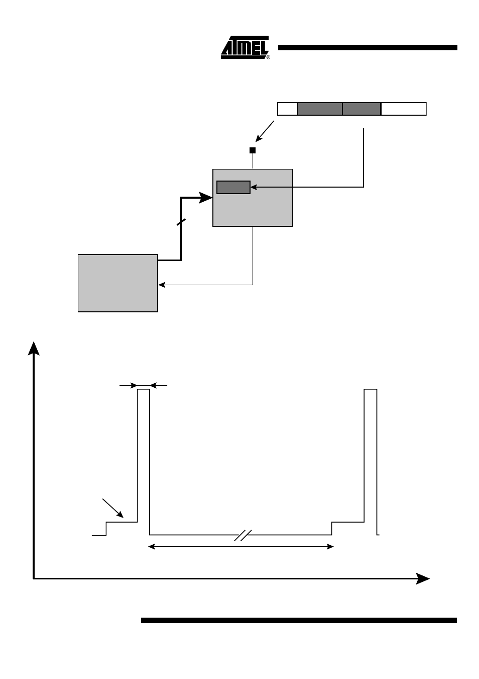
Figure 2. Wake-up Overview
Figure 3. Periodical Scan
Header + Address
Step 3: If a correct header is received (mandatory)
and address matches (if any), the data field
is then stored into AT86RF211 and WAKEUP pin is
activated (to wake-up the Microcontroller).
The Microcontroller will then read the data into one
of its registers, and begin a relevant procedure.
Note: Data field is optional: the chip can be simply
woken-up with no dedicated data.
AT86RF211 (TRX01)
Wake-up mode
3
Companion Microcontroller
WAKEUP pin
Step 2: The chip wakes-up periodically,
waiting for an expected message
(stand-alone operation)
Step 1: The chip is set up in sleep mode
using the 3-wire interface (SLE, SCK,
SDATA), then Microcontroller goes to sleep,
waiting for an interrupt on WAKEUP pin
Data stored
Data field
Reception mode
Short reception window
Oscillator settling
Sleep mode
Wake Up period
Timing
Power
Consumption
- RC2000 (2 pages)
- Т7023 (12 pages)
- Т7024 (20 pages)
- RC2200 (17 pages)
- RF01 (26 pages)
- RC1090 (17 pages)
- U3741BM (32 pages)
- U3742BM (32 pages)
- RAM01 (7 pages)
- RF22 (92 pages)
- RC1180-MBUS (28 pages)
- RFM01 (8 pages)
- RF12B (36 pages)
- RC1290 (17 pages)
- RC2300-ZNM (1 page)
- RF12 (31 pages)
- T48C862-R3 (107 pages)
- RF02 (24 pages)
- T48C862-R8 (107 pages)
- RFM12 (10 pages)
- U3745BM (29 pages)
- T5744 (19 pages)
- RFM12B (10 pages)
- U2745B (9 pages)
- T48C862-R4 (107 pages)
- RA01 (19 pages)
- T5754 (11 pages)
- U2741B (9 pages)
- RFM02 (8 pages)
- RC2100 (22 pages)
- RF модули диапазона ISM (4 pages)
- T5761 (35 pages)
- BTM -17х (5 pages)
- ATA8401 (12 pages)
- BTM -22х (7 pages)
- AT86RF231 (180 pages)
- ATA5575M1 (7 pages)
- AT88RF1354 (50 pages)
- ATA5812 (90 pages)
- AT86RF401 (50 pages)
- AT76C551 (77 pages)
- BTM -250 (6 pages)
- AT75C310 (132 pages)
- AT75C320 (13 pages)
- BTM -140 (6 pages)