Wake-up data rate register (wur) – Rainbow Electronics AT86RF211 User Manual
Page 38
38
AT86RF211
1942C–WIRE–06/02
•
WL2 programming
WL2 can be set as a multiple of WL1 from 0 to 31 WL1.
Wake-up Data Rate Register
(WUR)
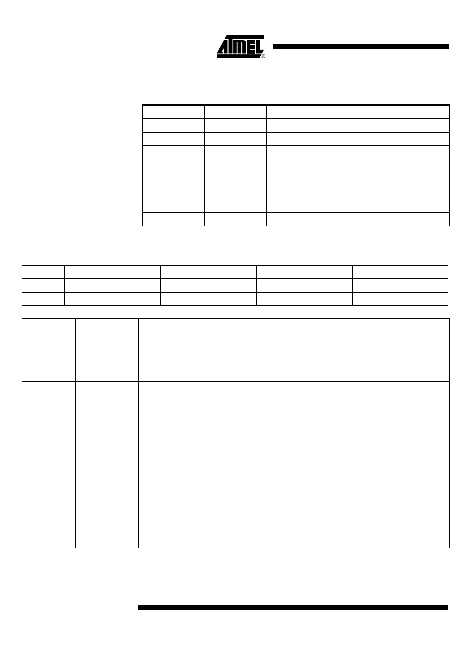
Table 18. WL2 Programming
WL2[2:0]
Period
Comments
(000)
2
0
Simultaneous test of the RSSI and the header
(001)
2
1 x WL1
(010)
2
2 x WL1
(011)
2
3 x WL1
(100)
2
4 x WL1
(101)
2
8 x WL1
(110)
2
16 x WL1
(111)
2
31 x WL1
Table 19. WUR Overview
Name
WUOP
RATECHK
RATE
RATETOL
nbit
17-16
15
14-5
4-0
init
(01)
2
0
(0000010000)
2
(01000)
2
Table 20. WUR Detailed Description
Name
Number of bits
Comments
WUOP
2
WAKEUP output polarity
(00)
2
: WAKEUP pin active low
(01)
2
: WAKEUP pin active high
(1x)
2
: WAKEUP pin open drain (active low, inactive tri-state)
reset value: (01)
2
RATECHK
1
Data rate check
the data rate is automatically extracted from the HEADER field.
the data rate can be compared to RATE with a tolerance of plus or minus RATETOL.
Data rate is computed from a unit of 1.56
µ
s (Reference clock divided by 16).
0: data rate not checked.
1: data rate check done (header ignored if check fails).
reset value: 0
RATE
10
Data rate value
0d: min value = 1 x 1.56 µs
(1023)
10
: max value = 1024 x 1.56 µs
reset value: 64 x 1.56
µ
s
reset value: (63)
10
RATETOL
5
Data rate tolerance
0d: min value = 0 x 1.56 µs
(31)
10
: max value = 31 x 1.56 µs
reset value: 8 x 1.56 µs
reset value: (8)
10