Rainbow Electronics AT86RF211 User Manual
Page 23
23
AT86RF211
1942C–WIRE–06/02
•
Register Interface Format
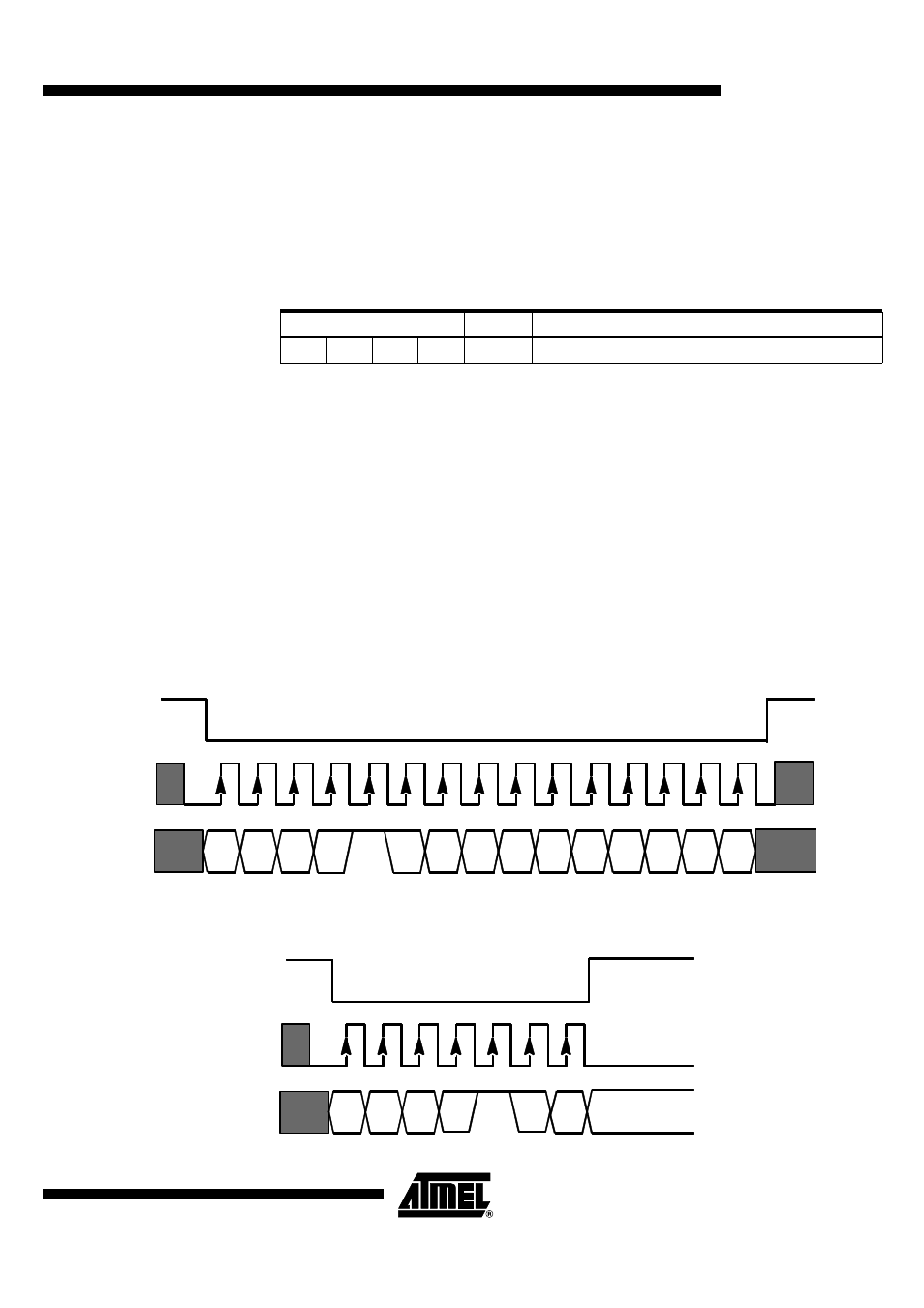
A message is made of 3 fields:
–
address A[3:0]: 4 bits (MSB first)
–
R/W: read/write selection
–
data D[31:0]: up to 32 bits (MSB first)
Variable register length and partial read or write cycles are supported.
In case of partial read or write cycles, the first data (in or out) is always the MSB of the
register.
•
WRITE Mode (R/W = 1)
The address, R/W and data bits are clocked on the rising edge of SCK.
If the number of data bits is lower than the register capacity, the LSB bits keep their
former value allowing safe partial write. If the number of data bits is greater than the reg-
ister capacity, the extra bits are ignored.
The data is actually written into the register on the rising edge of SLE when the data
length is less or equal to the register length.
When trying to write more data than the register length, data field is written on the first
extra rising clock edge regarding register length.
Figure 29. Write Chronogram: Complete Write Cycle in a 10 bits Register
The complete register of 10 bits is updated on a rising edge of SLE.
Figure 30. Write Chronogram: Partial Write Cycle, Writing 2 bits
ADDRESS
R/W
DATA up to 32 bits (variable length)
A[3]
A[2]
A[1]
A[0]
R/W
MSB
D[nbit-1:0]
LSB
D[8]
A[1]
A[2]
D[7]
A[3]
R / W
S L E
S C K
S D A T A
D[6]
D[5]
D[4]
D[3]
D[2]
D[1]
D[0]
A[0]
D[9]
A[1]
A[2]
A[3]
R / W
S L E
S C K
S D A T A
D[30]
A[0]
D[31]