Digital timing characteristics (continued) – Rainbow Electronics ATA5812 User Manual
Page 84
84
ATA5811/ATA5812 [Preliminary]
4689B–RKE–04/04
15.9
Time period SCK low to
CS high
33, 35
T
SCK_setup1
250
ns
C
15.10
Time period SCK low to
CS low
33, 35
T
SCK_setup2
250
ns
C
15.11
Time period CS low to
SCK high
33, 35
T
SCK_hold
250
ns
C
16
Start Time Push Button Tn and PWR_ON
Timing of wake-up via PWR_ON or Tn
16.1
PWR_ON high to
positive edge on pin
IRQ (see Figure 30 on
page 42)
From OFF mode to Idle
mode, applications
according to Figure 4
on page 6, Figure 5 on
page 7 and Figure 6 on
page 8
XTAL:
C
m
= 4..7 fF (typ. 5 fF)
C
0
< 2.2 pF (typ. 1.8 pF)
R
m
≤
120
Ω
(typ. 15
Ω
)
1-battery application
C
1
= C
2
= 68 nF
C
3
= C
4
= 68 nF
C
5
= 10 nF
2-battery application
C
1
= C
4
= 68 nF
C
2
= C
3
= 2.2 µF
C
5
= 10 nF
Car application
C
1
= C
3
= C
4
= 68 nF
C
2
= C
12
= 2.2 µF
C
5
= 10nF
29, 40
T
PWR_ON_IRQ_1
0.3
0.45
0.45
0.8
1.3
1.3
ms
B
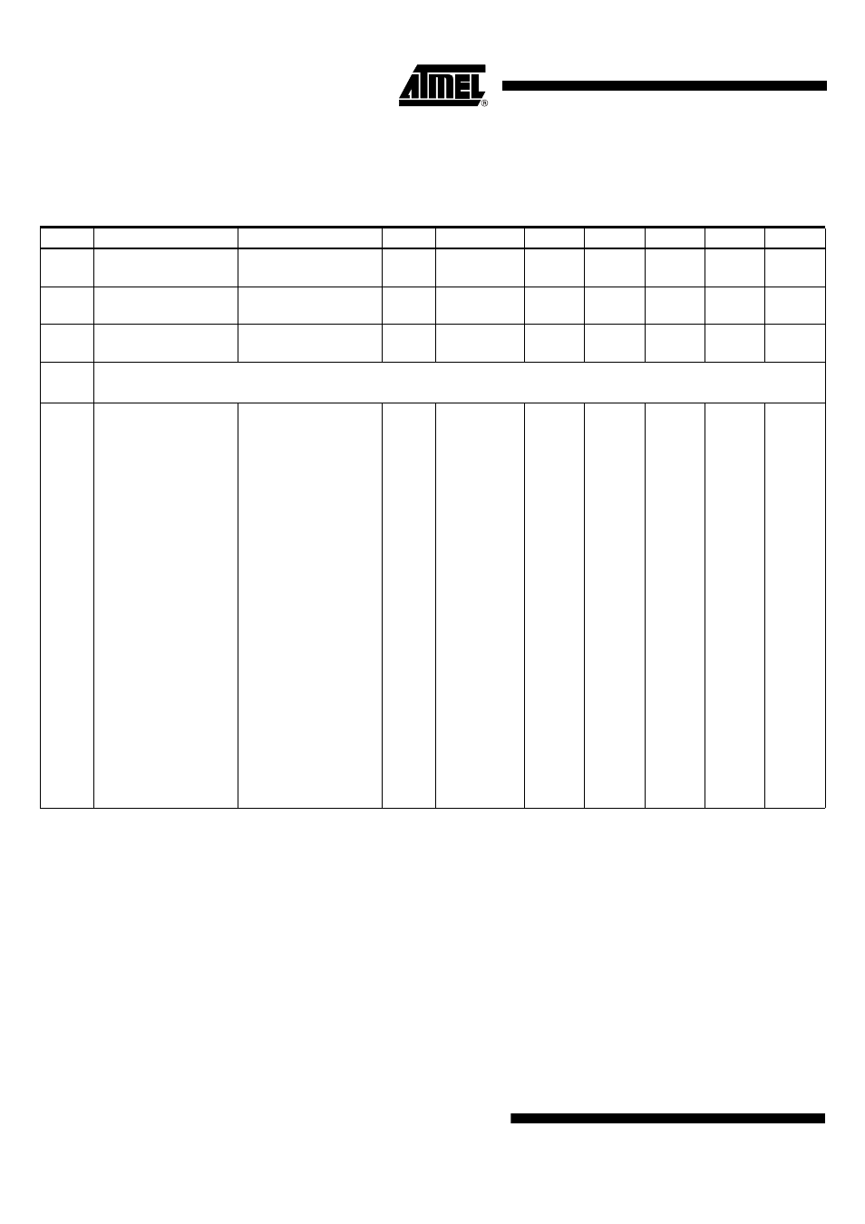
Digital Timing Characteristics (Continued)
All parameters refer to GND and are valid for T
amb
= -40°C to +105°C. V
VS1
= V
S2
= 2.4 V to 3.6 V (1-battery application),
V
V S 2
= 4.4 V to 6.6 V (2-batter y application) and V
V S 2
= 4.75 V to 5.25 V (car application), typical values at
V
VS1
= V
VS2
= 3 V and T
amb
= 25°C unless otherwise specified.
No.
Parameters
Test Conditions
Pin
Symbol
Min.
Typ.
Max.
Unit
Type*
*) Type means: A = 100% tested, B = 100% correlation tested, C = Characterized on samples, D = Design parameter