Transceiver configuration, Command: read tx/rx data buffer, Command: write tx/rx data buffer – Rainbow Electronics ATA5812 User Manual
Page 45: Command: read control/status register

45
ATA5811/ATA5812 [Preliminary]
4689B–RKE–04/04
Transceiver
Configuration
The configuration of the transceiver takes place via a 4-wire serial interface (CS, SCK,
SDI_TMDI, SDO_TMDO) and is organized in 8-bit units. The configuration is initiated
with a 8-bit command. While shifting the command into pin SDI_TMDI, the number of
bytes in the TX/RX data buffer are available on pin SDO_TMDO. The read and write
commands are followed by one or more 8-bit data units. Each 8-bit data transmission
begins with the MSB. The serial interface is in reset state if the level on pin CS = Low.
Command:
Read TX/RX Data Buffer
During a RX operation the user can read the received bytes in the TX/RX data buffer
successively.
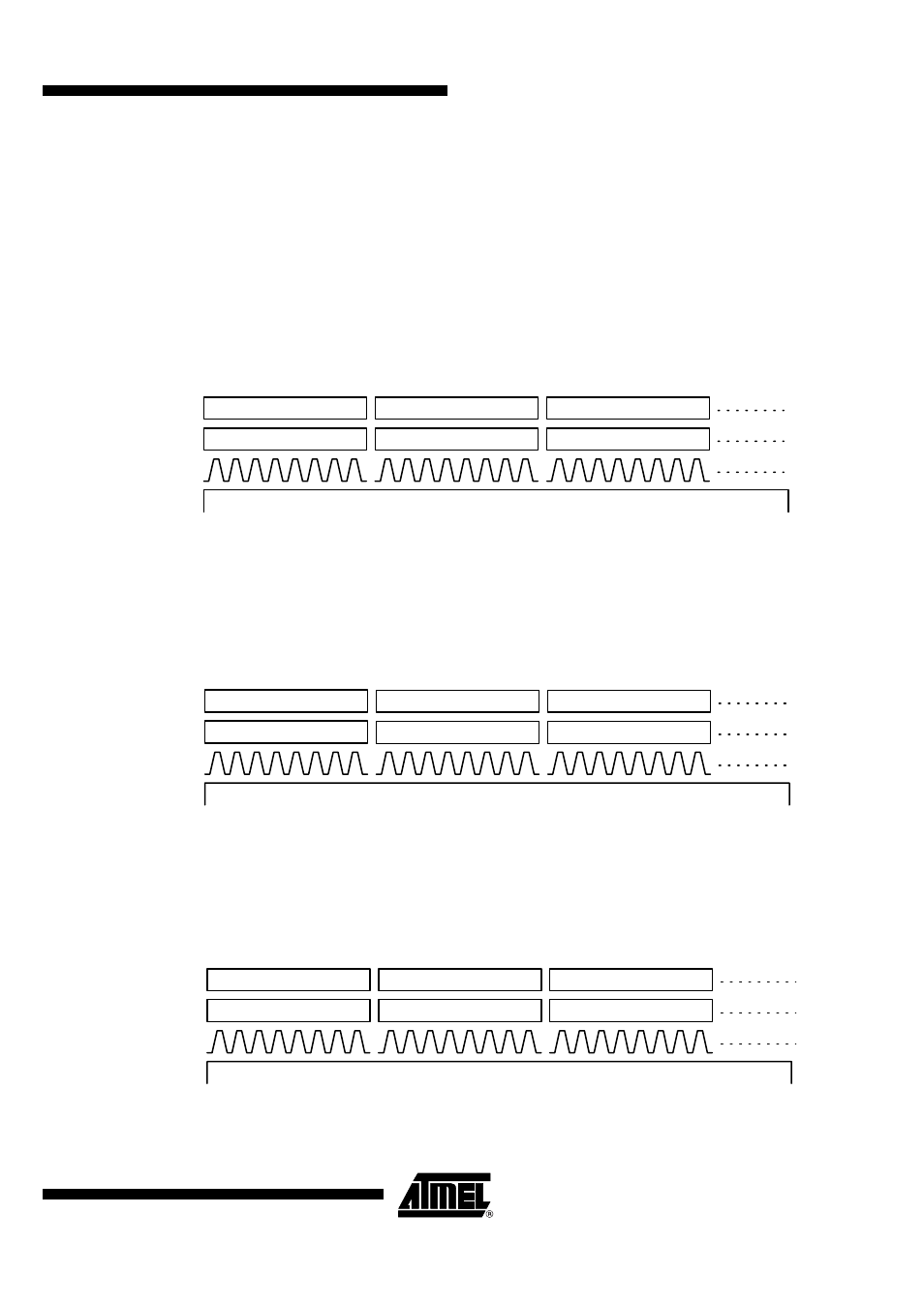
Figure 33. Read TX/RX Data Buffer
Command:
Write TX/RX Data Buffer
During a TX operation the user can write the bytes in the TX/RX data buffer succes-
sively. An echo of the command and the TX data bytes are provided for the
microcontroller on pin SDO_TMDO.
Figure 34. Write TX/RX Data Buffer
Command: Read
Control/Status Register
The control and status registers can be read individually or successively.
Figure 35. Read Control/Status Register
Command: Read TX/RX Data Buffer
SDI_TMDI
SDO_TMDO
Nr. Bytes in the TX/RX Data Buffer
SCK
X
RX Data Byte 1
X
RX Data Byte 2
CS
MSB
LSB
MSB
LSB
LSB
MSB
Command: Write TX/RX Data Buffer
SCK
TX Data Byte 1
TX Data Byte 2
Write TX/RX Data Buffer
TX Data Byte 1
SDI_TMDI
SDO_TMDO
CS
MSB
LSB
MSB
LSB
MSB
LSB
Nr. Bytes in the TX/RX Data Buffer
Command: Read C/S Register X
SCK
Data C/S Register X
SDI_TMDI
SDO_TMDO
CS
MSB
LSB
MSB
LSB
Nr. Bytes in the TX/RX Data Buffer
Data C/S Register Y
MSB
LSB
Command: Read C/S Register Y
Command: Read C/S Register Z
