Rainbow Electronics ATA5812 User Manual
Page 22

22
ATA5811/ATA5812 [Preliminary]
4689B–RKE–04/04
Note that if matching to 50
Ω
, like in Figure 5 on page 7, a high Q wire wound inductor
with a Q > 70 should be used for L
2
to minimize its contribution to RX losses which will
otherwise be dominant. The RX and TX losses will be in the range of 1.0 dB there.
XTO
The XTO is an amplitude regulated Pierce oscillator type with integrated load capaci-
tances (2
×
18 pF with a tolerance of ±17%) hence C
Lmin
= 7.4 pF and C
Lmax
= 10.6 pF.
The XTO oscillation frequency f
XTO
is the reference frequency FREF for the fractional-N
synthesizer. When designing the system in terms of receiving and transmitting fre-
quency offset the accuracy of the crystal and XTO have to be considered.
The synthesizer can adjust the local oscillator frequency for more than ±150 ppm at
433.92 MHz/315 MHz and up to ±118 ppm at 868.3 MHz of initial frequency error in
f
XTO
. This is done at nominal supply voltage and temperature
with the control registers 2
and 3 (see Table 20 on page 35 and Table 23 on page 36). The remaining local oscilla-
tor tolerance at nominal supply voltage and temperature is then < ±0.5 ppm. A XTO
frequency error of ±150 ppm/±118 ppm can hence be tolerated due to the crystal toler-
ance at 25°C and the tolerances of C
L1
and C
L2
. The XTO’s gm has very low influence of
less than ±2 ppm on the frequency at nominal supply voltage and temperature.
Over temperature and supply voltage, the XTO's additional pulling is only ±2 ppm if
C
m
≤
7
fF. The XTAL versus temperature and its aging is then the main source of fre-
quency error in the local oscillator.
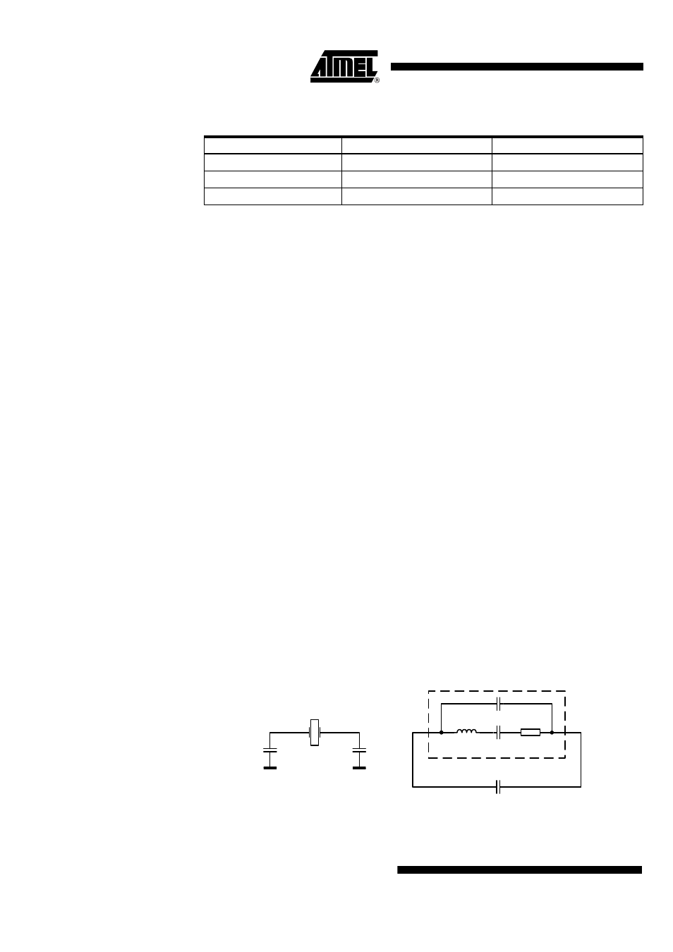
The XTO frequency depends on XTAL properties and the load capacitances C
L1, 2
at pin
XTAL1 and XTAL2. The pulling of f
XTO
from the nominal f
XTAL
is calculated using the fol-
lowing formula:
ppm.
C
m
is the crystal's motional, C
0
the shunt and C
LN
the nominal load capacitance of the
XTAL found in its data sheet. C
L
is the total actual load capacitance of the crystal in the
circuit and consists of C
L1
and C
L2
in series connection.
Figure 18. XTAL with Load Capacitance
Table 11. Impedance RF_OUT Pin in RX Mode
Frequency
Z(RF_OUT)RX
R
P
//C
P
315
MHz
36
Ω −
j
502
Ω
7 k
Ω / /
1.0 pF
433.92
MHz
19
Ω −
j
366
Ω
7 k
Ω / /
1.0 pF
868.3
MHz
2.8
Ω −
j 141
Ω
7 k
Ω / /
1.3 pF
P
C
m
2
--------
C
LN
C
L
–
C
0
C
LN
+
(
)
C
0
C
L
+
(
)
Ч
-------------------------------------------------------------
Ч
10
6
Ч
=
XTAL
C
L1
C
L2
C
0
C
m
L
m
R
m
C
L
= C
L1
C
L2
/(C
L1
+ (C
L2
)
Crystal equivalent circuit
Ч
