Rainbow Electronics ATA5812 User Manual
Page 50
50
ATA5811/ATA5812 [Preliminary]
4689B–RKE–04/04
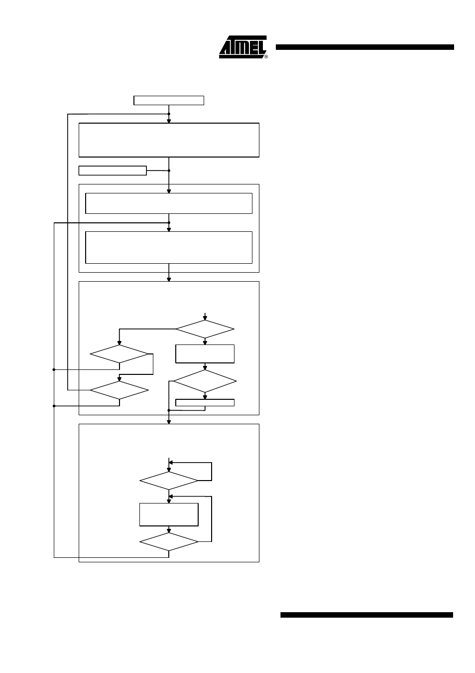
Figure 40. Flow Chart Polling Mode/RX Mode (T_MODE = 1, Transparent Mode Inactive)
Sleep mode:
All circuits for analog signal processing are disabled. Only XTO and Polling logic
is enabled.
Output level on pin RX_ACTIVE -> Low; I
S
= I
IDLE_X
T
Sleep
= Sleep
Ч
1024
Ч
T
DCLK
×
X
Sleep
Start-up signal processing:
The signal processing circuit are enabled.
Output level on pin RX_ACTIVE -> High; I
S
= I
RX_X
T
Startup_Sig_Proc
Bit-check mode:
The incomming data stream is analyzed. If the timing indicates a valid transmitter
signal, the control bits VSOUT_EN, CLK_ON and OPM0 are set to 1 and the
transceiver is set to receiving mode. Otherwise it is set to Sleep mode or to
Start-up mode.
Output level on Pin RX_ACTIVE -> High
I
S
= I
RX_X
T
Bit-check
Receiving mode:
The incomming data stream is passed via the TX/RX Data Buffer to the
connected microcontroller. If an bit error occurs the transceiver is set back to
Start-up mode.
Output level on pin RX_ACTIVE -> High
I
S
= I
RX_X
Start-up PLL:
The PLL is enabled and locked.
Output level on pin RX_ACTIVE -> High; I
S
= I
Startup_PLL_X
;T
Startup_PLL
Start-up mode:
OPM0 = 1
?
Bit check
OK ?
YES
NO
NO
YES
Set VSOUT_EN = 1
Set CLK_ON = 1
Set OPM0 = 1
Start bit
detected ?
YES
Sleep:
Defined by bits Sleep0 to Sleep4 in Control
Register 4
X
Sleep
:
Defined by bit XSleep in Control Register 4
T
DCLK
:
Basic clock cycle
T
Startup_PLL
:
798.5
×
T
DCLK
(typ)
T
Startup_Sig_Proc
:
882
×
T
DCLK
(BR_Range 0)
498
×
T
DCLK
(BR_Range 1)
306
×
T
DCLK
(BR_Range 2)
210
×
T
DCLK
(BR_Range 3)
Is defined by the selected baud rate range and
T
DCLK
. The baud-rate range is defined by bit
Baud0 and Baud1 in Control Register 6.
T
Bit-check
:
Depends on the result of the bit check.
If the bit check is ok, T
Bit-check
depends on the
number of bits to be checked (N
Bit-check
) and
on the utilized data rate.
If the bit check fails, the average time period for
that check depends on the selected baud-rate
range and on T
XDCLK
. The baud-rate range is
defined by bit Baud0 and Baud1 in Control
Register 6.
P_MODE = 0
?
YES
Set IRQ
NO
Start RX Polling Mode
Start RX Mode
RX data stream is
written into the TX/RX
Data Buffer
Bit error ?
YES
T
SLEEP
= 0
?
NO
YES
NO
NO
If the transceiver detects a bit error after a
successful bit check and before the start bit is
detected pin IRQ will be set to high (only if
P_MODE=0) and the transceiver is set back to
start-up mode.