Electrical characteristics: general (continued) – Rainbow Electronics ATA5812 User Manual
Page 67
67
ATA5811/ATA5812 [Preliminary]
4689B–RKE–04/04
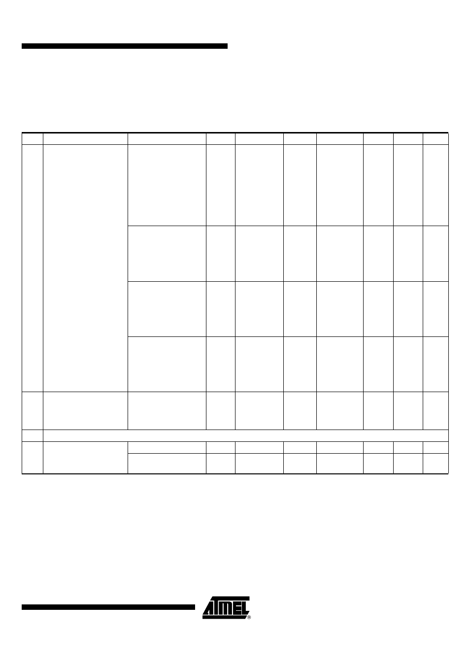
2.22 Blocking
Sensitivity (BER = 10
-3
)
is reduced by 6
dB if a
continuous wave
blocking signal at ±
∆
f is
∆
P
Block
higher than the
useful signal level
(baud rate = 20 kBaud,
FSK, f
DEV
±16kHz,
Manchester code)
f
RF
= 315 MHz
∆
f ± 0.75
MHz
∆
f ± 1.0
MHz
∆
f ± 1.5
MHz
∆
f ± 5
MHz
∆
f ± 10
MHz
(4)
∆
P
Block
56
60
63
69
71
dBC
C
f
RF
= 433.92 MHz
∆
f ± 0.75
MHz
∆
f ± 1.0
MHz
∆
f ± 1.5
MHz
∆
f ± 5
MHz
∆
f ± 10
MHz
(4)
∆
P
Block
55
59
62
68
70
dBC
C
f
RF
= 868.3 MHz
∆
f ± 0.75
MHz
∆
f ± 1.0
MHz
∆
f ± 1.5
MHz
∆
f ± 5
MHz
∆
f ± 10
MHz
(4)
∆
P
Block
50
53
57
67
69
dBC
C
2.23 CDEM
C
6
in
Figure 4 on page 6,
Figure 5 on page 7 and
Figure 6 on page 8
37
-5%
15
+5%
nF
D
3
Power Amplifier/TX Mode
3.1
Supply current TX mode
power amplifier OFF
f
RF
= 868.3
MHz
I
S_TX_PAOFF
6.50
mA
A
f
RF
= 433.92
MHz and
f
RF
= 315
MHz
I
S_TX_PAOFF
6.95
mA
A
Electrical Characteristics: General (Continued)
All parameters refer to GND and are valid for T
amb
= -40°C to +105°C, V
VS1
= V
VS2
= 2.4 V to 3.6 V (1-battery application),
V
VS2
= 4.4 V to 6.6 V (2-battery application) and V
VS2
= V
VAUX
= 4.75 V to 5.25 V (car application). Typical values are given
at V
VS1
= V
VS2
= 3 V and T
amb
= 25°C, f
RF
= 433.92 MHz (1-battery application) unless otherwise specified. Details about cur-
rent consumption, timing and digital pin properties can be found in the specific sections of the “Electrical Characteristics”.
No. Parameters
Test Conditions
Pin
(1)
Symbol
Min.
Typ.
Max.
Unit
Type*
*) Type means: A = 100% tested, B = 100% correlation tested, C = Characterized on samples, D = Design parameter
Note:
1. Pin numbers in brackets mean they were measured with RF_IN matched to 50
Ω
according to Figure 7 on page 10 with
component values according to Table 2 on page 10 and RF_OUT matched to 50
Ω
according to Figure 16 on page 19 with
component values according to Table 7 on page 19.