Figure 22: 3-wire interface. write command, hiz=0, Figure 23: 3-wire interface. write command, hiz=1, Figure 24: 3-wire interface. read command – Rainbow Electronics 71M6542G User Manual
Page 72
72
© 2008–2011 Teridian Semiconductor Corporation
v1.1
4
RD
W
Indicates that EEDATA (SFR 0x9E) is to be filled with data from EEPROM.
3:0
CNT[3:0]
W
Specifies the number of clocks to be issued. Allowed values are 0
through 8. If RD=1, CNT bits of data are read MSB first, and right
justified into the low order bits of EEDATA. If RD=0, CNT bits are sent
MSB first to the EEPROM, shifted out of the MSB of EEDATA. If
CNT[3:0] is zero, SDATA simply obeys the HiZ bit.
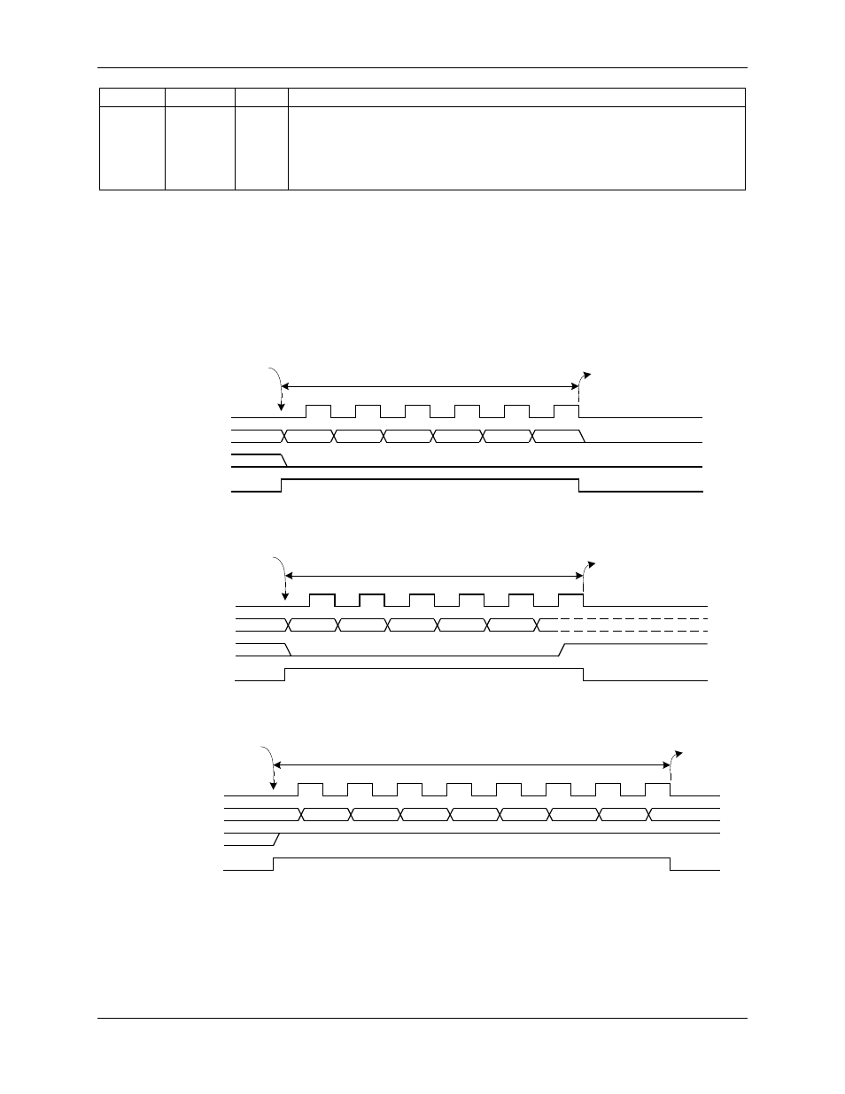
The timing diagrams in
through
describe the 3-wire EEPROM interface behavior. All
commands begin when the EECTRL (SFR 0x9F) register is written. Transactions start by first raising the
DIO pin that is connected to CS. Multiple 8-bit or less commands such as those shown in
through
are then sent via EECTRL and EEDATA.
When the transaction is finished, CS must be lowered. At the end of a Read transaction, the EEPROM is
driving SDATA, but transitions to Hi-Z (high impedance) when CS falls. The firmware should then
immediately issue a write command with CNT=0 and HiZ=0 to take control of SDATA and force it to a
low-Z state.
Figure 22: 3-wire Interface. Write Command, HiZ=0.
Figure 23: 3-wire Interface. Write Command, HiZ=1
Figure 24: 3-wire Interface. Read Command.
SCLK (output)
BUSY (bit)
CNT Cycles (6 shown)
SDATA (output)
Write -- No HiZ
D2
D3
D4
D5
D6
D7
EECTRL Byte Written
INT5
SDATA output Z
(LoZ)
CNT Cycles (6 shown)
Write -- With HiZ
INT5
EECTRL Byte Written
SCLK (output)
BUSY (bit)
SDATA (output)
D2
D3
D4
D5
D6
D7
(HiZ)
(LoZ)
SDATA output Z
CNT Cycles (8 shown)
READ
D0
D1
D2
D3
D4
D5
INT5
D6
D7
EECTRL Byte Written
SCLK (output)
BUSY (bit)
SDATA (input)
SDATA output Z
(HiZ)