13 vlcd generator, Vlcd generator, Table 109: lcd driver performance specifications – Rainbow Electronics 71M6542G User Manual
Page 146
146
© 2008–2011 Teridian Semiconductor Corporation
v1.1
6.4.13 VLCD Generator
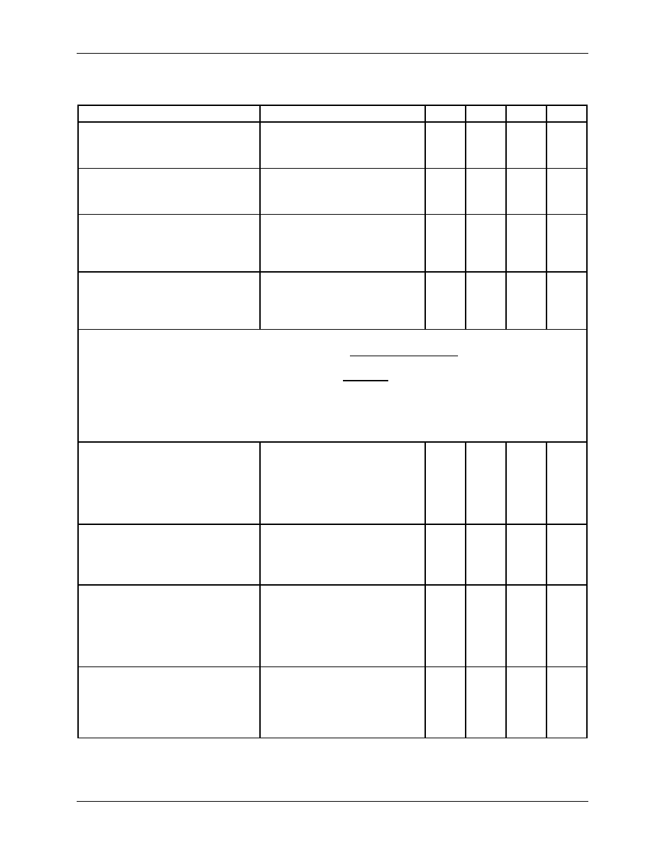
Table 108: LCD Driver Performance Specifications
Parameter
Condition
Min
Typ
Max
Unit
VSYS to VLCD switch impedance
V3P3 = 3.3 V,
RVLCD=removed, LCD_BAT=0,
LCD_VMODE[1:0]=0,
∆ILCD=10 µA
750
Ω
VBAT to VLCD switch impedance
V3P3 = 0 V, VBAT = 2.5 V,
RVLCD =removed, LCD_BAT =1,
LCD_VMODE[1:0]=0,
∆ILCD=10 µA
700
Ω
LCD Boost Frequency
LCD_VMODE[1:0] = 2,
RVLCD = removed,
CVLCD = removed
PLL_FAST=1
PLL_FAST=0
820
786
kHz
kHz
VLCD IOH current
(VLCD(0)-VLCD(IOH)<0.25)
LCD_VMODE[1:0] = 2,
LCD_CLK[1:0] = 2,
RVLCD = removed,
V3P3 = 3.3V,
LCD_DAC[4:0] = 1F
10
µA
From LCDADJ0 and LCDADJ12 fuses:
𝐿𝐶𝐷𝐴𝐷𝐽(𝐿𝐶𝐷_𝐷𝐴𝐶) = 5𝑚𝑉 �𝐿𝐶𝐷𝐴𝐷𝐽0 +
𝐿𝐶𝐷𝐴𝐷𝐽12 − 𝐿𝐶𝐷𝐴𝐷𝐽0
12
𝐿𝐶𝐷_𝐷𝐴𝐶�
𝑉𝐿𝐶𝐷
𝑁𝑂𝑀
(𝐿𝐶𝐷_𝐷𝐴𝐶) = 2.65 + 2.65
𝐿𝐶𝐷_𝐷𝐴𝐶
31
+ 𝐿𝐶𝐷𝐴𝐷𝐽(𝐿𝐶𝐷_𝐷𝐴𝐶)
The above equations describe the nominal value of VLCD for a specific LCD_DAC value. The
specifications below list the maximum deviation between actual VLCD and VLCDnom. Note that when
VCC and boost are insufficient, the LCD DAC will not reach its target value and a large negative error
will occur.
LCD_DAC Error. VLCD-VLCDnom
(see note 1)
Full Scale, with Boost
V3P3 =3.6 V
V3P3 =3.0 V
VBAT=4.0 V, V3P3=0, BRN Mode
VBAT=2.5 V, V3P3=0, BRN Mode
LCD_VMODE[1:0] = 2,
LCD_DAC[4:0] = 1F,
LCD_CLK[1:0]=2,
LCD_MODE[2:0]=6
-0.15
-0.4
-0.15
-1.3
0.15
0.15
0.15
V
V
V
V
LCD_DAC Error. VLCD-VLCDnom
DAC=12, with Boost
V3P3 = 3.6 V
V3P3 = 3.0 V
VBAT = 2.5 V, V3P3 = 0 V, BRN Mode
LCD_VMODE[1:0] = 2,
LCD_DAC[4:0] = C,
LCD_CLK[1:0]=2,
LCD_MODE[2:0]=6
-0.15
-0.15
-0.15
0.15
0.15
0.15
V
V
V
LCD_DAC Error. VLCD-VLCDnom
Zero Scale, with Boost
V3P3 = 3.6 V
V3P3 = 3.0 V
VBAT = 4.0 V, V3P3 = 0 V, BRN Mode
(see note 1)
VBAT = 2.5 V, V3P3 = 0 V, BRN Mode
LCD_VMODE[1:0] = 2,
LCD_DAC[4:0] =0,
LCD_CLK[1:0]=2,
LCD_MODE[2:0]=6
-0.15
-0.15
-0.15
-0.15
0.15
0.15
0.15
0.15
V
V
V
V
LCD_DAC Error. VLCD-VLCDnom
Full Scale, no Boost
V3P3 = 3.6 V (see note 1)
V3P3 = 3.0 V (see note 1)
VBAT = 4.0 V, V3P3 = 0 V, BRN Mode
VBAT = 2.5 V, V3P3 = 0 V, BRN Mode
LCD_VMODE[1:0] = 1,
LCD_DAC[4:0] = 1F,
LCD_CLK[1:0]=2,
LCD_MODE[2:0]=6
-2.1
-2.8
-1.8
-3.2
V
V
V
V