2 digital i/o for the 71m6541d/f, Table 48 – Rainbow Electronics 71M6542G User Manual
Page 61
v1.1
© 2008–2011 Teridian Semiconductor Corporation
61
2.5.8.2 Digital I/O for the 71M6541D/F
A total of 32 combined SEG/DIO pins plus 5 SEG outputs are available for the 71M6541D/F. These pins
can be categorized as follows:
17 combined SEG/DIO segment pins:
o
SEGDIO4…SEGDIO5 (2 pins)
o
SEGDIO9…SEGDIO14 (6 pins)
o
SEGDIO19…SEGDIO25 (7 pins)
o
SEGDIO44…SEGDIO45 (2 pins)
15 combined SEG/DIO segment pins shared with other functions:
o
SEGDIO0/WPULSE, SEGDIO1/VPULSE (2 pins)
o
SEGDIO2/SDCK, SEGDIO3/SDATA (2 pins)
o
SEGDIO6/XPULSE, SEGDIO7/YPULSE (2 pins)
o
SEGDIO8/DI (1 pin)
o
SEGDIO26/COM5, SEGDIO27/COM4 (2 pins)
o
SEGDIO36/SPI_CSZ…SEGDIO39/SPI_CKI (4 pins)
o
SEGDIO51/OPT_TX, SEGDIO55/OPT_RX (2 pins)
5 dedicated SEG segment pins are available:
o
ICE Inteface pins: SEG48/E_RXTX, SEG49/E_TCLK, SEG50/E_RST (3 pins)
o
Test Port pins: SEG46/TMUX2OUT, SEG47/TMUXOUT (2 pins)
There are four dedicated common segment outputs (COM0…COM3) plus the two additional shared common
segment outputs that are listed under combined SEG/DIO shared pins (SEGDIO26/COM5,
SEGDIO27/COM4).
Thus, in a configuration where none of these pins are used as DIOs, there can be up to 37 LCD segment
pins with 4 commons, or 35 LCD segment pins with 6 commons. And in a configuration where LCD
segment pins are not used, there can be up to 32 DIO pins.
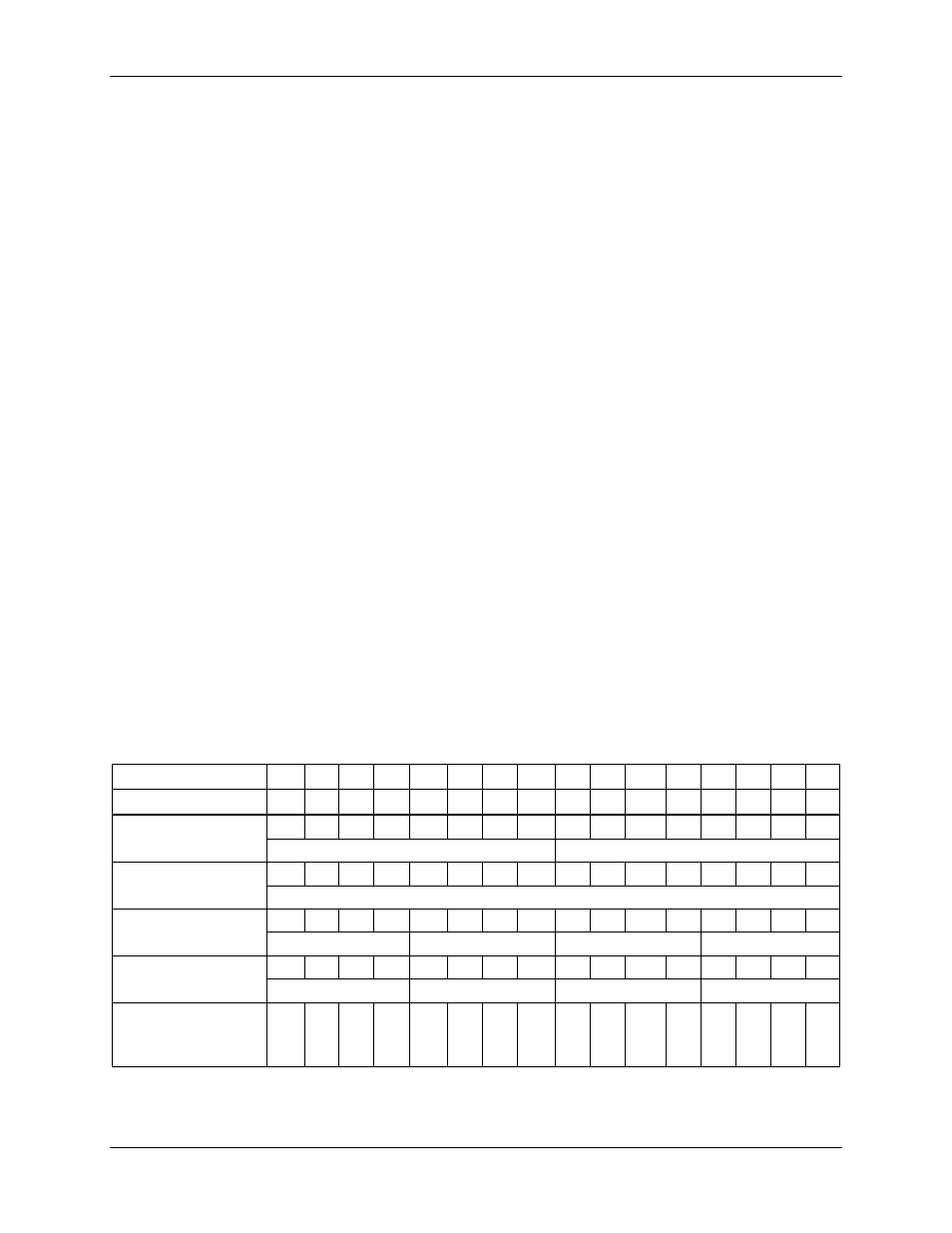
The configuration for pins SEGDIO19 to SEGDIO27 is shown in
, and the configuration for pins
SEGDIO36-39 and SEGDIO44-45 is shown in
. SEG46 to SEG50 cannot be configured for DIO.
The configuration for pins SEGDIO51 and SEGDIO55 is shown in
Table 48: Data/Direction Registers for SEGDIO0 to SEGDIO14 (71M6541D/F)
SEGDIO
0
1
2
3
4
5
6
7
8
9
10
11 12 13 14 15
Pin #
31
30 29
28 27
26 25
24
23 22
21
20 19 18 17
–
Configuration:
0 = DIO, 1 = LCD
0
1
2
3
4
5
6
7
0
1
2
3
4
5
6
–
LCD_MAP[7:0] (I/O RAM 0x240B)
LCD_MAP[14:8] (I/O RAM 0x240A)
SEG Data Register
0
1
2
3
4
5
6
7
8
9
10
11 12 13 14
–
LCD_SEG0[5:0] to LCD_SEG14[5:0] (I/O RAM 0x2410[5:0] to 0x241E[5:0]
DIO Data Register
0
1
2
3
0
1
2
3
0
1
2
3
0
1
2
–
P0 (SFR 0x80)
P1 (SFR 0x90)
P2 (SFR 0xA0)
P3 (SFR 0xB0)
Direction Register:
0 = input, 1 = output
4
5
6
7
4
5
6
7
4
5
6
7
4
5
6
–
P0 (SFR 0x80)
P1 (SFR 0x90)
P2 (SFR 0xA0)
P3 (SFR 0xB0)
Internal Resources
Configurable
(see
–
–
Y
Y
Y
Y
Y
Y
Y
Y
Y
Y
–
–
–
–