Preliminary – Rainbow Electronics T89C51CC02 User Manual
Page 89
Rev.A - May 17, 2001
89
Preliminary
T89C51CC02
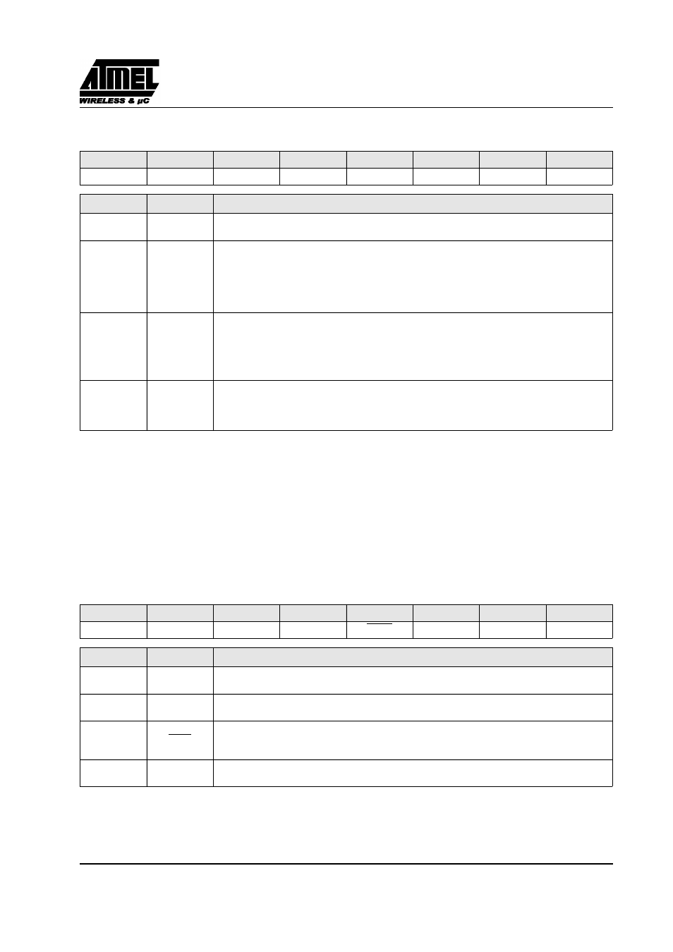
CANBT3 (S:B6h)
CAN Bit Timing Registers 3
Note:
The CAN controller bit timing registers must be accessed only if the CAN controller is disabled with the ENA bit of the CANGCON register set to 0.
See Figure 60.
No default value after reset.
Figure 76. CANBT3 Register
CANPAGE (S:B1h)
CAN message object Page Register
Reset Value: 0000 0000b
Figure 77. CANPAGE Register
7
6
5
4
3
2
1
0
-
PHS2 2
PHS2 1
PHS2 0
PHS1 2
PHS1 1
PHS1 0
SMP
Bit Number Bit Mnemonic
Description
7
-
Reserved
The value read from this bit is indeterminate. Do not set this bit.
6-4
PHS2 2:0
Phase segment 2
This phase is used to compensate for phase edge errors. This segment can be shortened by the re-
synchronization jump width.
3-1
PHS1 2:0
Phase segment 1
This phase is used to compensate for phase edge errors. This segment can be lengthened by the re-
synchronization jump width.
0
SMP
Sample type
0 - once, at the sample point.
1 - three times, the threefold sampling of the bus is the sample point and twice over a distance of a
1/2 period of the Tscl. The result corresponds to the majority decision of the three values.
7
6
5
4
3
2
1
0
-
-
CHNB 1
CHNB 0
AINC
INDX2
INDX1
INDX0
Bit Number Bit Mnemonic
Description
7-6
-
Reserved
The value read from these bit are indeterminate. Do not set these bits.
5-4
CHNB1:0
Selection of message object number
The available numbers are: 0 to 3 (see Figure 57).
3
AINC
Auto increment of the index (active low)
0 - auto-increment of the index (default value).
1 - non-auto-increment of the index.
2-0
INDX2:0
Index
Byte location of the data field for the defined message object (see Figure 57).
Tphs2
Tscl
PHS2 2
…
0
]
[
1
+
(
)
×
=
Tphs1
Tscl
PHS1 2
…
0
]
[
1
+
(
)
Ч
=