internal space, lower 128 bytes ram, upper 128 bytes ram – Rainbow Electronics T89C51CC02 User Manual
Page 29: expanded ram, Preliminary, Internal space
Rev.A - May 17, 2001
29
Preliminary
T89C51CC02
8.2. Internal Space
8.2.1. Lower 128 Bytes RAM
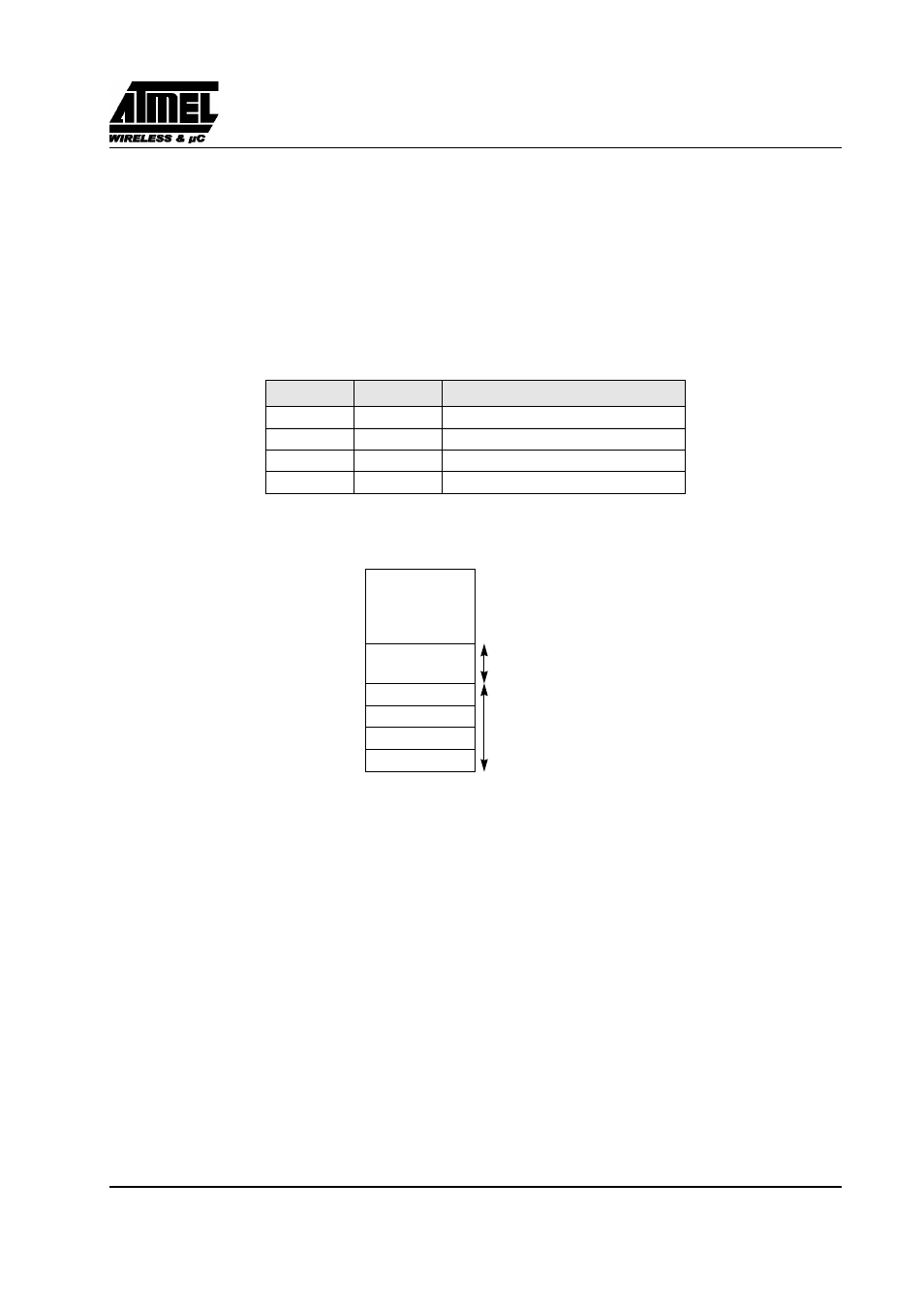
The lower 128 bytes of RAM (see Figure 13) are accessible from address 00h to 7Fh using direct or indirect
addressing modes. The lowest 32 bytes are grouped into 4 banks of 8 registers (R0 to R7). Two bits RS0 and RS1
in PSW register (see Figure 16) select which bank is in use according to Table 15. This allows more efficient use
of code space, since register instructions are shorter than instructions that use direct addressing, and can be used
for context switching in interrupt service routines.
Table 15. Register Bank Selection
The next 16 bytes above the register banks form a block of bit-addressable memory space. The C51 instruction
set includes a wide selection of single-bit instructions, and the 128 bits in this area can be directly addressed by
these instructions. The bit addresses in this area are 00h to 7Fh.
Figure 14. Lower 128 bytes Internal RAM Organization
8.2.2. Upper 128 Bytes RAM
The upper 128 bytes of RAM are accessible from address 80h to FFh using only indirect addressing mode.
8.2.3. Expanded RAM
The on-chip 256 bytes of expanded RAM (ERAM) are accessible from address 0000h to FFh using indirect
addressing mode through MOVX instructions.
Caution:
Lower 128 bytes RAM, Upper 128 bytes RAM, and expanded RAM are made of volatile memory cells. This means that the RAM content is
indeterminate after power-up and must then be initialized properly.
RS1
RS0
Description
0
0
Register bank 0 from 00h to 07h
0
1
Register bank 0 from 08h to 0Fh
1
0
Register bank 0 from 10h to 17h
1
1
Register bank 0 from 18h to 1Fh
Bit-Addressable Space
4 Banks of
8 Registers
R0-R7
30h
7Fh
(Bit Addresses 0-7Fh)
20h
2Fh
18h
1Fh
10h
17h
08h
0Fh
00h
07h