registers, Preliminary, Registers – Rainbow Electronics T89C51CC02 User Manual
Page 31
Rev.A - May 17, 2001
31
Preliminary
T89C51CC02
8.4. Registers
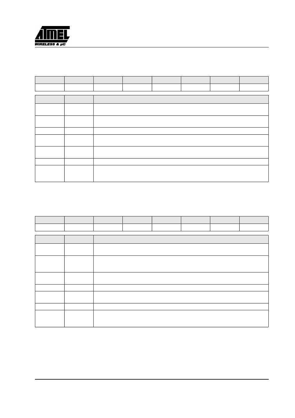
PSW (S:8Eh)
Program Status Word Register.
Reset Value= 0000 0000b
Figure 16. PSW Register
AUXR1 (S:A2h)
Auxiliary Control Register 1.
Reset Value= XXXX 00X0b
Figure 17. AUXR1 Register
7
6
5
4
3
2
1
0
CY
AC
F0
RS1
RS0
OV
F1
P
Bit Number Bit Mnemonic
Description
7
CY
Carry Flag
Carry out from bit 1 of ALU operands.
6
AC
Auxiliary Carry Flag
Carry out from bit 1 of addition operands.
5
F0
User Definable Flag 0.
4-3
RS1:0
Register Bank Select Bits
Refer to Table 15 for bits description.
2
OV
Overflow Flag
Overflow set by arithmetic operations.
1
F1
User Definable Flag 1.
0
P
Parity Bit
Set when ACC contains an odd number of 1’s.
Cleared when ACC contains an even number of 1’s.
7
6
5
4
3
2
1
0
-
-
ENBOOT
-
GF3
0
-
DPS
Bit Number Bit Mnemonic
Description
7-6
-
Reserved
The value read from these bits is indeterminate. Do not set these bits.
5
ENBOOT
Enable Boot Flash
Set this bit for map the boot flash between F800h -FFFFh
Clear this bit for disable boot flash.
4
-
Reserved
The value read from this bit is indeterminate. Do not set this bit.
3
GF3
General Purpose Flag 3.
2
0
Always Zero
This bit is stuck to logic 0 to allow INC AUXR1 instruction without affecting GF3 flag.
1
-
Reserved for Data Pointer Extension.
0
DPS
Data Pointer Select Bit
Set to select second dual data pointer: DPTR1.
Clear to select first dual data pointer: DPTR0.