Preliminary – Rainbow Electronics T89C51CC02 User Manual
Page 115
Rev.A - May 17, 2001
115
Preliminary
T89C51CC02
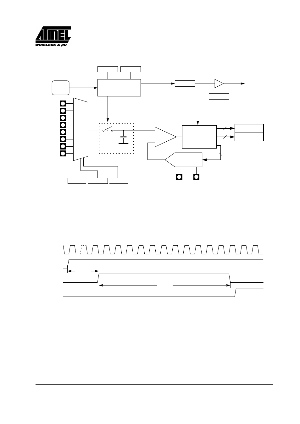
Figure 117. ADC Description
Figure 118 shows the timing diagram of a complete conversion. For simplicity, the figure depicts the waveforms
in idealized form and do not provide precise timing information. For ADC characteristics and timing parameters
refer to the Section “AC Characteristics” of the T89C51CC02 datasheet.
Figure 118. Timing Diagram
NOTE:
Tsetup = 4 us
Tconv=11 clock ADC
AN0/P1.0
AN1/P1.1
AN2/P1.2
AN3/P1.3
AN4/P1.4
AN5/P1.5
AN6/P1.6
AN7/P1.7
000
001
010
011
100
101
110
111
SCH2
ADCON.2
SCH0
ADCON.0
SCH1
ADCON.1
ADC
CLOCK
ADEN
ADCON.5
ADSST
ADCON.3
ADEOC
ADCON.4
ADC
Interrupt
Request
EADC
IEN1.1
CONTROL
AVSS
Sample and Hold
ADDH
VAREF
R/2R DAC
VAGND
8
10
+
-
ADDL
2
SAR
ADCIN
ADEN
ADSST
ADEOC
T
SETUP
T
CONV
CLK
See also other documents in the category Rainbow Electronics Sensors:
- MAX5151 (16 pages)
- MAXQ3108 (64 pages)
- MAX5661 (39 pages)
- MAX6691 (7 pages)
- MAX5362 (12 pages)
- ADC10158 (26 pages)
- MAX8922L (14 pages)
- MAX8596Z (8 pages)
- MAX7491 (18 pages)
- MAX15040 (15 pages)
- MAX5177 (16 pages)
- ADC08138 (22 pages)
- MAX5961 (42 pages)
- T89C51RD2 (86 pages)
- MAX16055 (9 pages)
- MAX6659 (17 pages)
- ADC0820 (20 pages)
- MAX6678 (19 pages)
- MAX8884Z (15 pages)
- MAX16915 (9 pages)
- MAX8620 (18 pages)
- MAX5144 (12 pages)
- MAX6670 (8 pages)
- MAX8760 (39 pages)
- W78C32C (14 pages)
- MX7533 (8 pages)
- MAX8727 (13 pages)
- MAX9053 (15 pages)
- W78C54 (16 pages)
- MAX8614B (15 pages)
- W90N740 (219 pages)
- MAX6626 (13 pages)
- ADC10738 (30 pages)
- MAX17000 (31 pages)
- MAX5051 (21 pages)
- MAXQ1004 (18 pages)
- MAX6871 (51 pages)
- MX7847 (12 pages)
- MAX6608 (6 pages)
- MAX17083 (15 pages)
- MAX6641 (17 pages)
- MAX5251 (16 pages)
- MAX6338 (8 pages)
- MAX6690 (16 pages)
- MAX8668 (18 pages)