flash memory architecture, fm0 memory architecture, Preliminary – Rainbow Electronics T89C51CC02 User Manual
Page 18
18
Rev.A - May 17, 2001
Preliminary
T89C51CC02
7.2. FLASH Memory Architecture
T89C51CC02 features two on-chip flash memories:
•
Flash memory FM0:
containing 16 Kbytes of program memory (user space) organized into 128 byte pages,
•
Flash memory FM1:
2 Kbytes for boot loader and Application Programming Interfaces (API).
The FM0 supports both parallel programming and Serial In-System Programming (ISP) whereas FM1 supports
only parallel programming by programmers. The ISP mode is detailed in the "In-System Programming" section.
All Read/Write access operations on FLASH Memory by user application are managed by a set of API described
in the "In-System Programming" section.
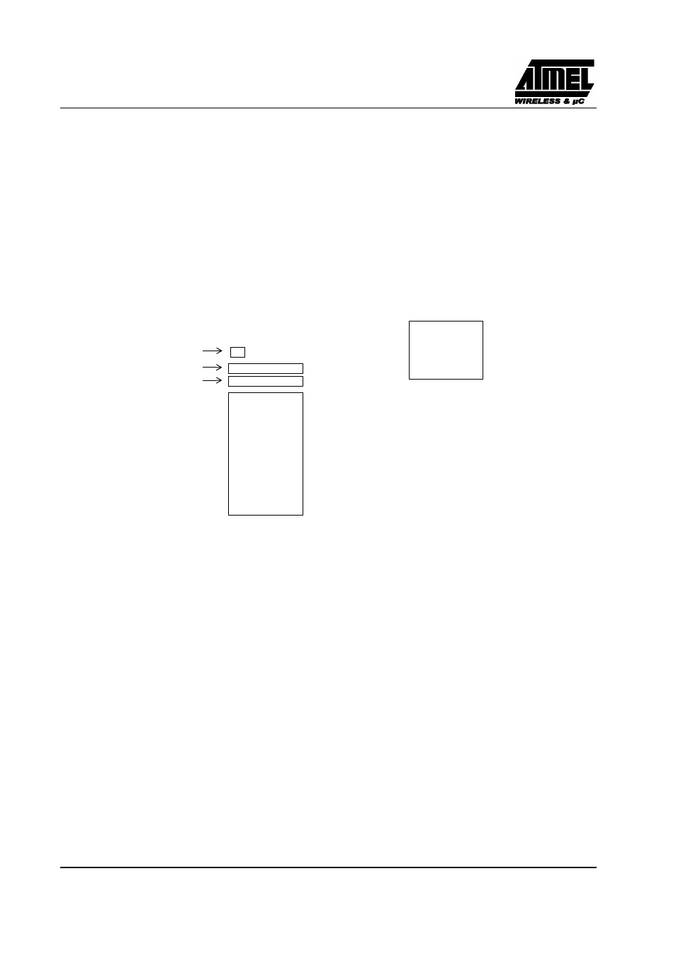
Figure 7. Flash memory architecture
7.2.1. FM0 Memory Architecture
The flash memory is made up of 4 blocks (see Figure 7):
1. The memory array (user space) 16 Kbytes
2. The Extra Row
3. The Hardware security bits
4. The column latch registers
7.2.1.1. User Space
This space is composed of a 16 Kbytes FLASH memory organized in 128 pages of 128 bytes. It contains the
user’s application code.
7.2.1.2. Extra Row (XRow)
This row is a part of FM0 and has a size of 128 bytes. The extra row may contain information for boot loader usage.
3FFFh
16 Kbytes
Flash memory
FM0
0000h
Hardware Security (1 byte)
Column Latches (128 bytes)
user space
Extra Row (128 bytes)
2 Kbytes
Flash memory
FM1
boot space
FFFFh
F800h
FM1 mapped between FFFFh and
F800h when bit ENBOOT is set in
AUXR1 register