i/o configurations, port structure, Preliminary – Rainbow Electronics T89C51CC02 User Manual
Page 6: I/o configurations, Port structure
6
Rev.A - May 17, 2001
Preliminary
T89C51CC02
4.1. I/O Configurations
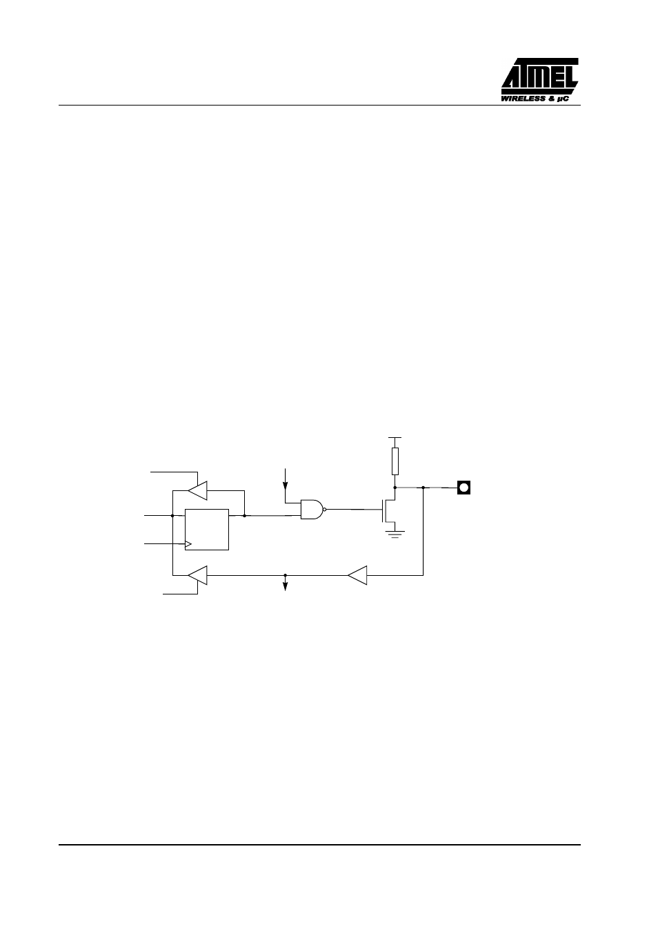
Each Port SFR operates via type-D latches, as illustrated in Figure 1 for Ports 3 and 4. A CPU "write to latch"
signal initiates transfer of internal bus data into the type-D latch. A CPU "read latch" signal transfers the latched
Q output onto the internal bus. Similarly, a "read pin" signal transfers the logical level of the Port pin. Some Port
data instructions activate the "read latch" signal while others activate the "read pin" signal. Latch instructions are
referred to as Read-Modify-Write instructions. Each I/O line may be independently programmed as input or output.
4.2. Port Structure
Figure 1 shows the structure of Ports 1 and 3, which have internal pull-ups. An external source can pull the pin
low. Each Port pin can be configured either forgeneral-purpose I/O or for its alternate input output function.
To use a pin for general-purpose output, set or clear the corresponding bit in the Px register (x=1,3 or 4). To use
a pin for general purpose input, set the bit in the Px register. This turns off the output FET drive.
To configure a pin for its alternate function, set the bit in the Px register. When the latch is set, the "alternate
output function" signal controls the output level (see Figure 1). The operation of Ports 1, 3 and 4 is discussed
further in "quasi-Bidirectional Port Operation" paragraph.
NOTE:
1. The internal pull-up can be disabled on P1 when analog function is selected.
Figure 1. Port Structure
D
CL
Q
LATCH
INTERNAL
WRITE
TO
LATCH
READ
PIN
READ
LATCH
Port.x
Port.X
ALTERNATE
OUTPUT
FUNCTION
VCC
INTERNAL
PULL-UP (1)
ALTERNATE
INPUT
FUNCTION
BUS