Bit timer/counter register description, Timer/counter control register – tccr0, Figure 42 – Rainbow Electronics ATmega8515L User Manual
Page 87: Figure 43, Atmega8515(l)

87
ATmega8515(L)
2512A–AVR–04/02
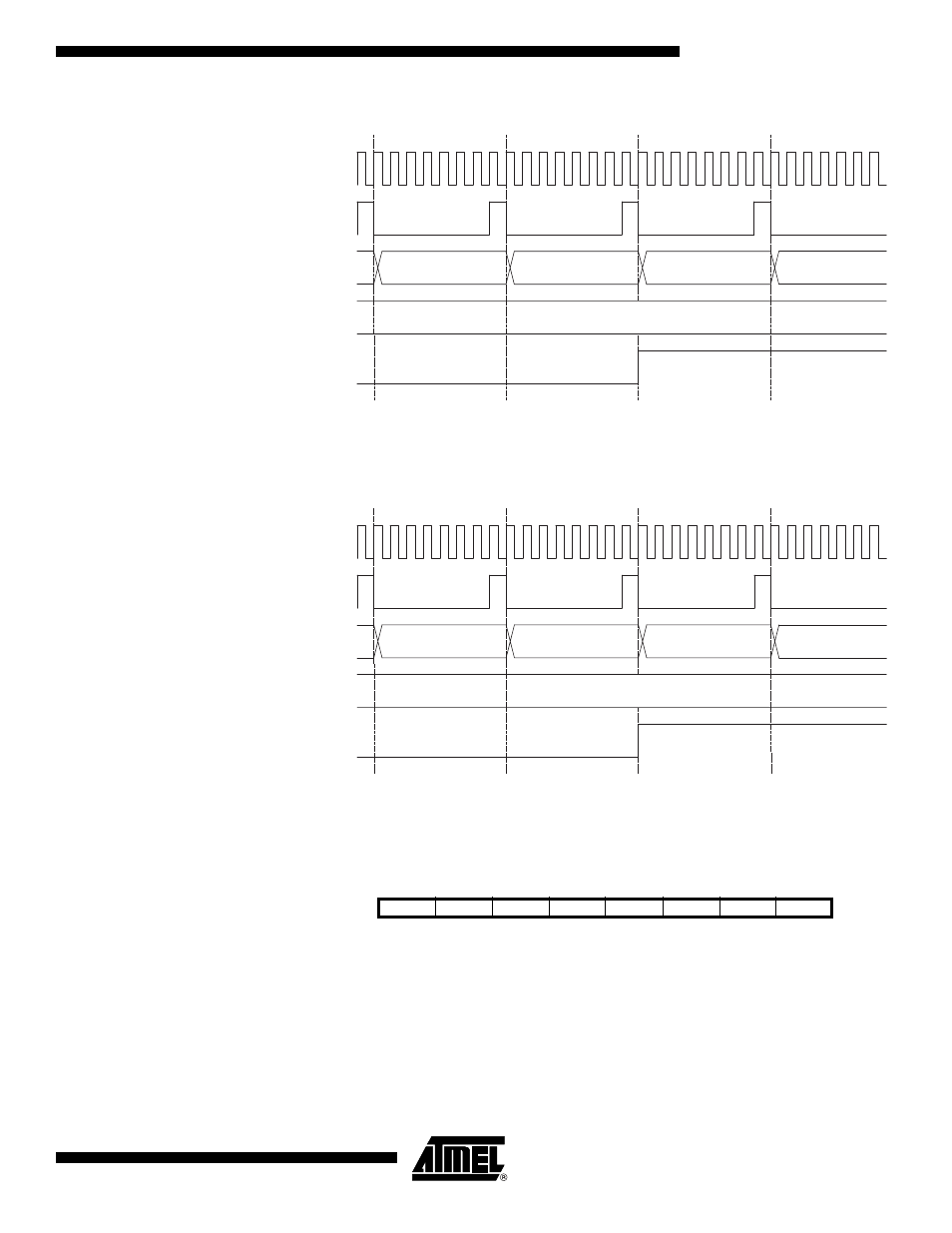
Figure 42. Timer/Counter Timing Diagram, Setting of OCF0, with Prescaler (f
clk_I/O
/8)
Figure 43 shows the setting of OCF0 and the clearing of TCNT0 in CTC mode.
Figure 43. Timer/Counter Timing Diagram, Clear Timer on Compare Match Mode, with
Prescaler (f
clk_I/O
/8)
8-bit Timer/Counter
Register Description
Timer/Counter Control
Register – TCCR0
• Bit 7 – FOC0: Force Output Compare
The FOC0 bit is only active when the WGM00 bit specifies a non-PWM mode. However,
for ensuring compatibility with future devices, this bit must be set to zero when TCCR0 is
written when operating in PWM mode. When writing a logical one to the FOC0 bit, an
immediate compare match is forced on the waveform generation unit. The OC0 output is
changed according to its COM01:0 bits setting. Note that the FOC0 bit is implemented
OCFn
OCRn
TCNTn
OCRn Value
OCRn - 1
OCRn
OCRn + 1
OCRn + 2
clk
I/O
clk
Tn
(clk
I/O
/8)
OCFn
OCRn
TCNTn
(CTC)
TOP
TOP - 1
TOP
BOTTOM
BOTTOM + 1
clk
I/O
clk
Tn
(clk
I/O
/8)
Bit
7
6
5
4
3
2
1
0
FOC0
WGM00
COM01
COM00
WGM01
CS02
CS01
CS00
TCCR0
Read/Write
W
R/W
R/W
R/W
R/W
R/W
R/W
R/W
Initial Value
0
0
0
0
0
0
0
0
