Atmega8515(l), Dc characteristics (continued) – Rainbow Electronics ATmega8515L User Manual
Page 195
195
ATmega8515(L)
2512A–AVR–04/02
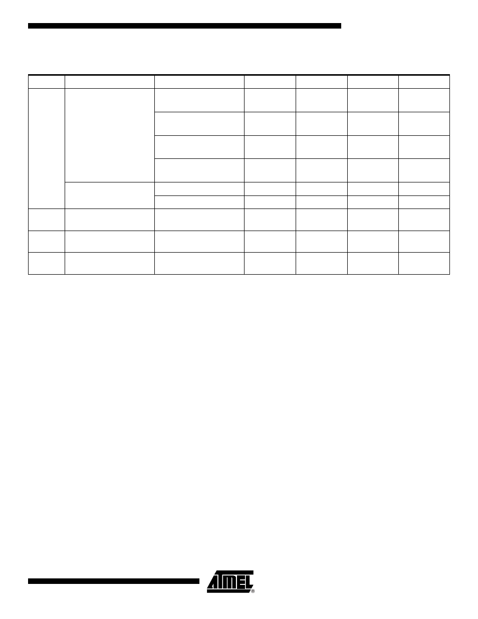
Notes:
1. “Max” means the highest value where the pin is guaranteed to be read as low.
2. “Min” means the lowest value where the pin is guaranteed to be read as high.
3. Although each I/O port can sink more than the test conditions (20 mA at V
CC
= 5V, 10 mA at V
CC
= 3V) under steady state
conditions (non-transient), the following must be observed:
1] The sum of all IOL, for all ports, should not exceed 300 mA.
2] The sum of all IOL, for ports B0 - B7, D0 - D7, and XTAL2, should not exceed 150 mA.
3] The sum of all IOL, for ports A0 - A7, E0 - E2, and C0 - C7 should not exceed 150 mA.
4. Although each I/O port can source more than the test conditions (20 mA at V
CC
= 5V, 10 mA at V
CC
= 3V) under steady state
conditions (non-transient),the following must be observed:
1] The sum of all IOH,for all ports,should not exceed 300 mA.
2] The sum of all IOH,for ports B0 - B7, D0 - D7, and XTAL2,should not exceed 150 mA.
3] The sum of all IOH,for ports A0 - A7, E0 - E2, and C0 - C7 should not exceed 150 mA.
5. Minimum V
CC
for Power-down is 2.5V.
I
CC
Power Supply Current
Active 4 MHz, V
CC
= 3V
(
ATmega8515
L)
3
mA
Active 8 MHz, V
CC
= 5V
(
ATmega8515
)
11
mA
Idle 4 MHz, V
CC
= 3V
(
ATmega8515
L)
1.5
mA
Idle 8 MHz, V
CC
= 5V
(
ATmega8515
)
5.5
mA
Power-down mode
WDT enabled, V
CC
= 3V
< 1
µA
WDT disabled, V
CC
= 3V
< 10
µA
V
ACIO
Analog Comparator
Input Offset Voltage
V
CC
= 5V
V
in
= V
CC
/2
40
mV
I
ACLK
Analog Comparator
Input Leakage Current
V
CC
= 5V
V
in
= V
CC
/2
-50
50
nA
t
ACID
Analog Comparator
Propagation Delay
V
CC
= 2.7V
V
CC
= 4.0V
750
500
ns
DC Characteristics (Continued)
T
A
= -40
°C to 85°C, V
CC
= 2.7V to 5.5V (Unless Otherwise Noted)
Symbol
Parameter
Condition
Min
Typ
Max
Units