Prom read timing – Intel 21555 User Manual
Page 85
21555 Non-Transparent PCI-to-PCI Bridge User Manual
85
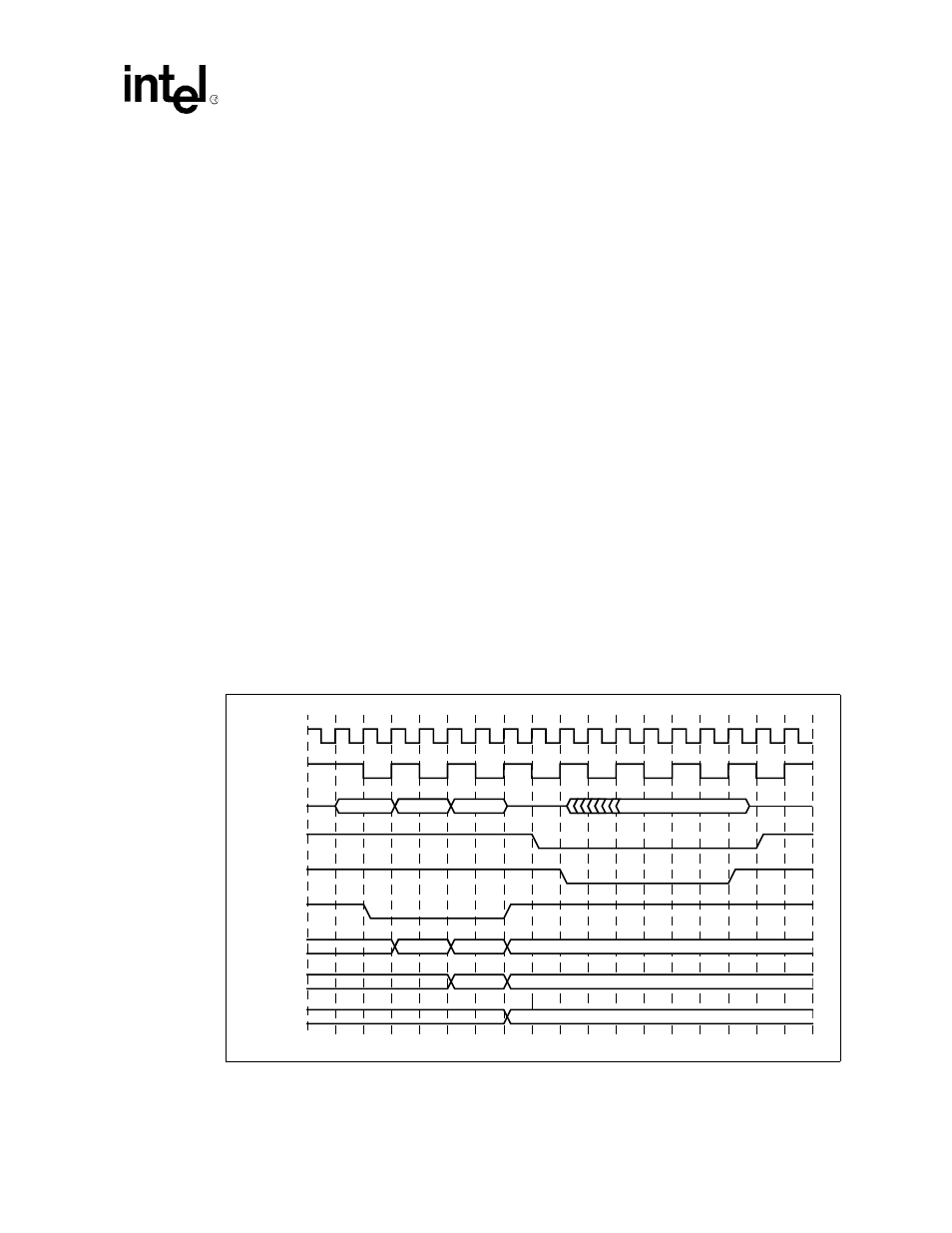
Parallel ROM Interface
When a byte read of the PROM is performed, the 21555 follows this sequence on the ROM interface, also shown in
1. The 21555 drives address bits [23:16] on the pr_ad[7:0] pins and asserts pr_ale_l to enable the address
registers.
2. The 21555 drives pr_clk high, latching address bits [23:16] into the first external register.
3. The 21555 drives pr_clk low.
4. The 21555 drives address bits [15:8] on the pr_ad[7:0] pins.
5. The 21555 drives pr_clk high, latching address bits [15:8] into the first external register, and address bits
[23:16] into the second external register.
6. The 21555 drives pr_clk low.
7. The 21555 drives address bits [7:0] on the pr_ad[7:0] pins.
8. The 21555 drives pr_clk high, latching address bits [7:0] into the first external register, address bits [15:8] into
the second external register, and address bits [23:16] into the third external register. All the ROM address bits
are now driven to the appropriate ROM pins.
9. The 21555 deasserts the address register enable, pr_ale_l.
10. The 21555 asserts the pr_cs_l and pr_rd_l pins according to the strobe setup timing specified by the Strobe
Mask in the ROM Setup register.
11. The PROM drives read data onto the pr_ad[7:0] pins.
12. The 21555 samples the read data and deasserts pr_rd_l as specified by the strobe mask. The 21555 also
deasserts pr_cs_l according to the access time specified in the ROM Setup register.
13. The 21555 clears the PROM Start bit in the
Table 112, “ROM Control Register” on page 178
.
14. Valid data can now be read from the ROM Data register.
.
Figure 15. PROM Read Timing
A7456-01
p_clk
pr_clk
pr_ad[7:0]
d[7:0]
pr_cs_l
pr_rd_l
pr_ale_l
a[7:0]
a[15:8]
a[23:16]
A3
A2
Read Data [7:0]
A1
A3
A2
A1 = Address[7:00]
A3
A2 = Address[15:8]
A3 = Address[23:16]