Intel 21555 User Manual
Page 161
21555 Non-Transparent PCI-to-PCI Bridge User Manual
161
List of Registers
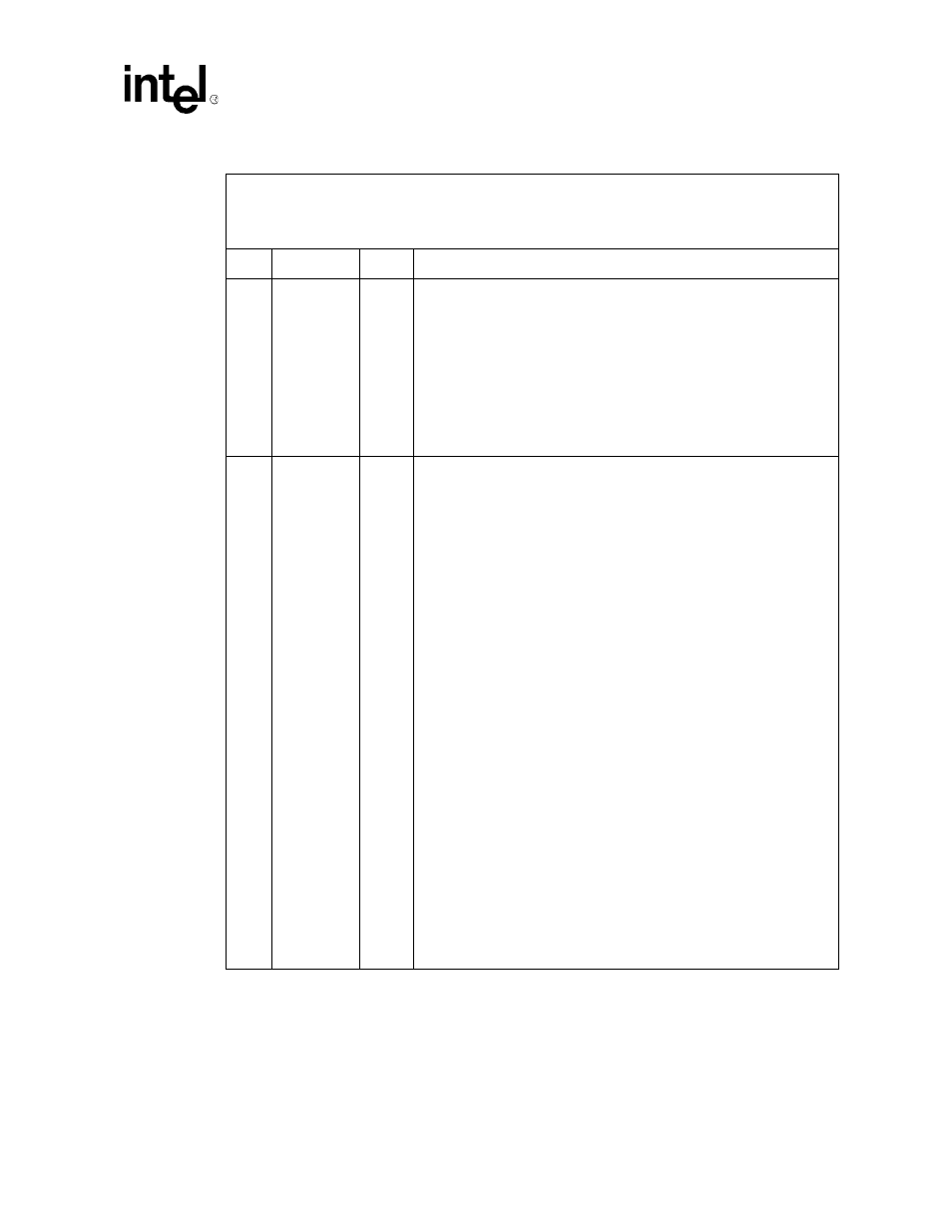
7:6
Subtractive
Decode
Enable
R/W
Controls subtractive decoding for downstream and upstream I/O
transactions. When the 21555 is enabled to perform subtractive decoding
in one direction, those transactions are forwarded to the opposite bus with
no address translation.
Possible values are:
•
00: No subtractive decoding is performed on either interface.
•
01: I/O subtractive decoding enabled on primary interface.
•
10: I/O subtractive decoding enabled on secondary interface.
•
11: Illegal. Results are unpredictable.
Reset value is 00
11:8
Page Size
R/W
Selects the page size used for the Upstream Memory 2 address range. The
total size of this range is dependent on the page size. Possible page size
values and their encoding are dependent on the LUT Page Size Extension
bit [12] in the Chip Control 0 register.
When the LUT Page Size Extension bit is 0, the encodings are:
•
0h : Disables the Upstream Memory 2 Base address register.
•
1h : 256 bytes
•
2h : 512 bytes
•
3h : 1 KB
•
4h : 2 KB
•
5h : 4 KB
•
6h : 8 KB
•
7h : 16 KB
•
8h : 32 KB
•
9h : 64 KB
•
Ah : 128 KB
•
Bh : 256 KB
•
Ch : 512 KB
•
Dh : 1 MB
•
Eh : 2 MB
•
Fh : 4 MB
When the LUT Page Size Extension bit is 1, the encodings are:
•
0h : Disables the Upstream Memory 2 Base address register.
•
1h : 8 MB
•
2h : 16 MB
•
3h : 32 MB
•
4h to Fh : Disables the Upstream Memory 2 Base address register.
Reset value is 0h
Table 78. Chip Control 1 Register (Sheet 2 of 3)
This register may be preloaded by serial ROM or programmed by the local processor before host
configuration.
•
Primary byte offset: CF:CEh
•
Secondary byte offset: CF:CEh
Bit
Name
R/W
Description