2 power and ground signals, 3 clock and system control signals, Power and ground signals -4 – Motorola MC68VZ328 User Manual
Page 46: Clock and system control signals -4, Figure 2-2, Typical crystal connection -4
2-4
MC68VZ328 User’s Manual
Clock and System Control Signals
2.2
Power and Ground Signals
The MC68VZ328 microprocessor has three types of power pins. They are V
DD
, V
SS
, and LV
DD
.
•
V
DD
—External power supply to drive all I/O pins and for the internal voltage regulator. It is
recommended to place a 0.1 µF bypass capacitor close to each of these pins.
•
V
SS
—Signal return pin for both digital and analog circuits.
•
LV
DD
—Internal voltage regulator output signal that is used by the internal circuitry. The LV
DD
pins
should not be used as an external circuit power supply due to current supply limitations. Each
package has unique bypass capacitor requirements. The TQFP package requires that an external
bypass capacitor circuit of 0.01
µ
F and 0.0001 µF (in parallel) be placed close to each of the LV
DD
pins, except pin 35, which requires a 270 nF and a 0.0001 µF
bypass capacitor. The PBGA has a
single LV
DD
pin (M1) requiring only a 270 nF and a 0.0001 µF
bypass capacitor.
NOTE:
For maximum noise immunity, ensure that external bypass capacitors are
placed as close to the pins as possible.
2.3
Clock and System Control Signals
There are four clock and system control signals.
•
EXTAL—External Clock/Crystal. This input signal connects to the external low frequency crystal.
The MC68VZ328 microprocessor supports both a 32.768 kHz and a 38.4 kHz crystal frequency.
For a 32.768 kHz input, the internal phase-locked loop generates a PLLCLK signal that passes
through two prescalers, and the resulting output (DMACLK and SYSCLK) clock is 16.58 MHz.
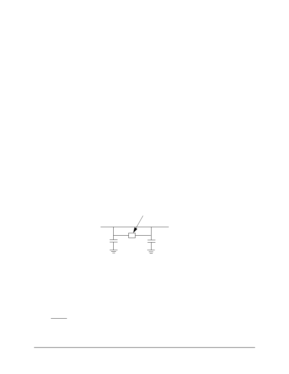
Figure 2-2 illustrates how a crystal is usually connected to the MC68VZ328. For specific circuit
design values, see Figure 4-2 on page 4-4.
Figure 2-2. Typical Crystal Connection
•
XTAL—Crystal. This output signal connects the on-chip oscillator output to an external crystal.
•
CLKO/PF2—Clock Out or bit 2 of Port F. This output clock signal is derived from the on-chip clock
oscillator and is internally connected to the clock output of the internal CGM. This signal is
provided for external reference. The output can be disabled in the PLL control register to reduce
power consumption and electromagnetic emission. See Section 4.4.1, “PLL Control Register,” on
page 4-8 for more information. The CLKO/PF2 signal defaults to the Port F pin 2 input signal. For
detailed information, refer to Section 10.4.7.3, “Port F Dedicated I/O Functions,” on page 10-26.
•
RESET—Reset. This active low, Schmitt trigger input signal resets the entire MC68VZ328
processor (CPU and peripherals). The threshold of this Schmitt trigger device is 1.2 V high and
0.8 V low. After the MC68VZ328 powers up, this reset input signal should be driven low for at least
EXTAL
XTAL
32.768
k
H
z
or 38.4
k
H
z
C2
C1