3 port b dedicated i/o functions, 4 port b pull-up enable register, Port b dedicated i/o functions -10 – Motorola MC68VZ328 User Manual
Page 180: Port b pull-up enable register -10, Table 10-9, Port b dedicated function assignments -10
10-10
MC68VZ328 User’s Manual
Programming Model
10.4.2.3
Port B Dedicated I/O Functions
The eight PBDATA lines are multiplexed with the chip-select, DRAM control, TIN/TOUT, and PWM
dedicated I/O signals whose assignments are shown in Table 10-9.
Bits 1–5 operate as chip-select signals or DRAM signals. Signal selection is controlled by bit 9 (DRAM) in
the chip-select D (CSD) register, which is described in Section 6.3.3, “Chip-Select Registers,” on page 6-8.
Bit 0 is used only as D0 or CSB0. No additional programming is required.
The TIN/TOUT line can be specified as either timer-input or timer-output by programming bit 6 in the
PBDIR register. Clearing the bit makes the line TIN. Setting the bit to 1 makes it TOUT. Unlike other port
register pins, the TOUT/TIN/PB6 pin direction is still controlled by the DIR6 bit in the Port B register even
though the pin is assigned to the GP timers. Refer to Section 12.1.4, “TOUT/TIN/PB6 Pin,” on page 12-3
for details about the operation and programming of the pin.
The PWMO1 signal is an output signal resulting from the logical operation (AND or OR) of both the
PWM 1 and PWM 2 modules. Bits 3–2 (P[1:0]) of the peripheral control register (PCR) select the logic
used for combining the modules. The PB7/PWMO1 pin defaults to a GPIO input pulled high. Refer to
Chapter 15, “Pulse-Width Modulator 1 and 2,” for additional information.
10.4.2.4
Port B Pull-up Enable Register
The Port B pull-up enable register (PBPUEN) controls the pull-up resistors for each line in Port B. The
settings for the bit positions are shown in Table 10-10 on page 10-11.
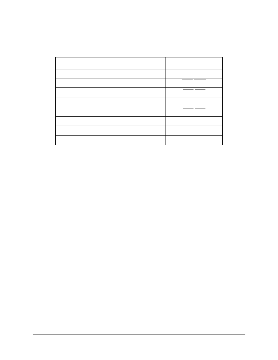
Table 10-9. Port B Dedicated Function Assignments
Bit
GPIO Function
Dedicated I/O Functions
0
Data bit 0
CSB0
1
Data bit 1
CSB1/SDWE
2
Data bit 2
CSC0/RAS0
3
Data bit 3
CSC1/RAS1
4
Data bit 4
CSD0/CAS0
5
Data bit 5
CSD1/CAS1
6
Data bit 6
TIN/TOUT
7
Data bit 7
PWMO1