Table 7-9, Sdram bank address programming examples -17 – Motorola MC68VZ328 User Manual
Page 127
Programming Model
DRAM Controller
7-17
BNKADDL
Bits 3–2
SDRAM Low Order Bank Address Line
Selection—A 2-bit bank register selection address is
generated by selecting the appropriate CPU address
line. This register bit allows selection of the low order
bit.
00 = PA19.
01 = PA21.
10 = PA23.
11 = Force this bank address line to 0.
See Table 7-9 for programming examples.
CL
Bit 1
CAS Latency—This bit selects the CAS latency for the
SDRAM cycle. The bit must be programmed before the
initialization sequence.
0 = CAS latency is 1 clock count.
1 = CAS latency is 2 clock counts.
RACL
Bit 0
Refresh to Active Command Latency—This bit
selects the latency for SDRAM from refresh to active
cycle.
0 = 3 Clock counts.
1 = 6 Clock counts.
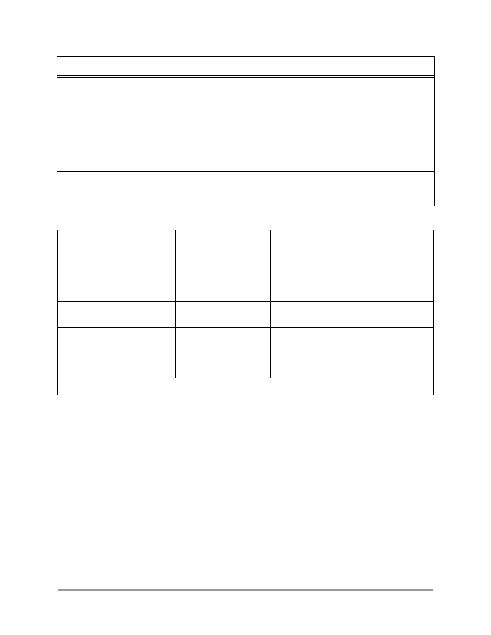
Table 7-9. SDRAM Bank Address Programming Examples
Application
BNKADDH
BNKADDL
Remarks
Make all SDRAM appear as one
single bank
11
11
None
Two banks of SDRAM—for exam-
ple, 16 Mbyte
00
11
Choose PA20 as bank selection address
Four banks of SDRAM—for
example, 64 Mbyte
01
10
Choose PA22 and PA21 as bank selection
address
Four banks of SDRAM—for
example, 128 Mbyte
01
10
Choose PA22 and PA23 as bank selection
address
Four banks of SDRAM—for
example, 256 Mbyte
10
10
Choose PA24 and PA23 as bank selection
address
Note:
These bits are all set in EDO RAM or Fast Page Mode, allowing the use of only one page register.
Table 7-8. SDRAM Control Register Description (Continued)
Name
Description
Setting