26 spi 1 and spi 2 generic timing, 27 spi 1 master using data_ready edge trigger, Spi 1 and spi 2 generic timing -32 – Motorola MC68VZ328 User Manual
Page 348: Spi 1 master using data_ready edge trigger -32, Figure 19-28 spi 1 master using
19-32
MC68VZ328 User’s Manual
AC Electrical Characteristics
19.3.26
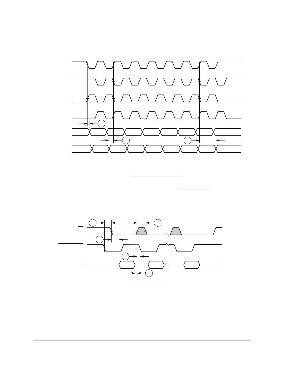
SPI 1 and SPI 2 Generic Timing
Figure 19-27 shows the timing diagram for SPI 1 and SPI 2. The signal values and units of measure for
Figure 19-27 through Figure 19-32 are found in Table 19-17 on page 19-34. Detailed information about
the operation of individual signals can be found in Chapter 13, “Serial Peripheral Interface 1 and 2.”
Figure 19-27. SPI 1 and SPI 2 Generic Timing Diagram
19.3.27
SPI 1 Master Using DATA_READY Edge Trigger
Figure 19-28 shows the timing diagram for the SPI 1 master using the DATA_READY edge trigger. The
signal values and units of measure for Figure 19-27 through Figure 19-32 are found in Table 19-17 on
page 19-34. Detailed information about the operation of individual signals can be found in Chapter 13,
“Serial Peripheral Interface 1 and 2.”
Figure 19-28. SPI 1 Master Using DATA_READY Edge Trigger Timing Diagram
SPICLK
(POL=1, PHA=1)
SPICLK
(POL=1, PHA=0)
SPICLK
(POL=0, PHA=1)
SPICLK
(POL=0, PHA=0)
TxD/MOSI
RxD/MISO
1
Bn
Bn–1
Bn–2
Bn–3
B1
B0
Bn
Bn–1
Bn–2
Bn–3
B1
B0
2
3
SS
(Output)
DATA_READY
(Input)
SCLK,
MOSI, MISO
5
7
4
8
6