4 chip-select flash write cycle timing, Chip-select flash write cycle timing -6, Table 19-5 – Motorola MC68VZ328 User Manual
Page 322: Chip-select write cycle timing parameters -6
19-6
MC68VZ328 User’s Manual
AC Electrical Characteristics
19.3.4
Chip-Select Flash Write Cycle Timing
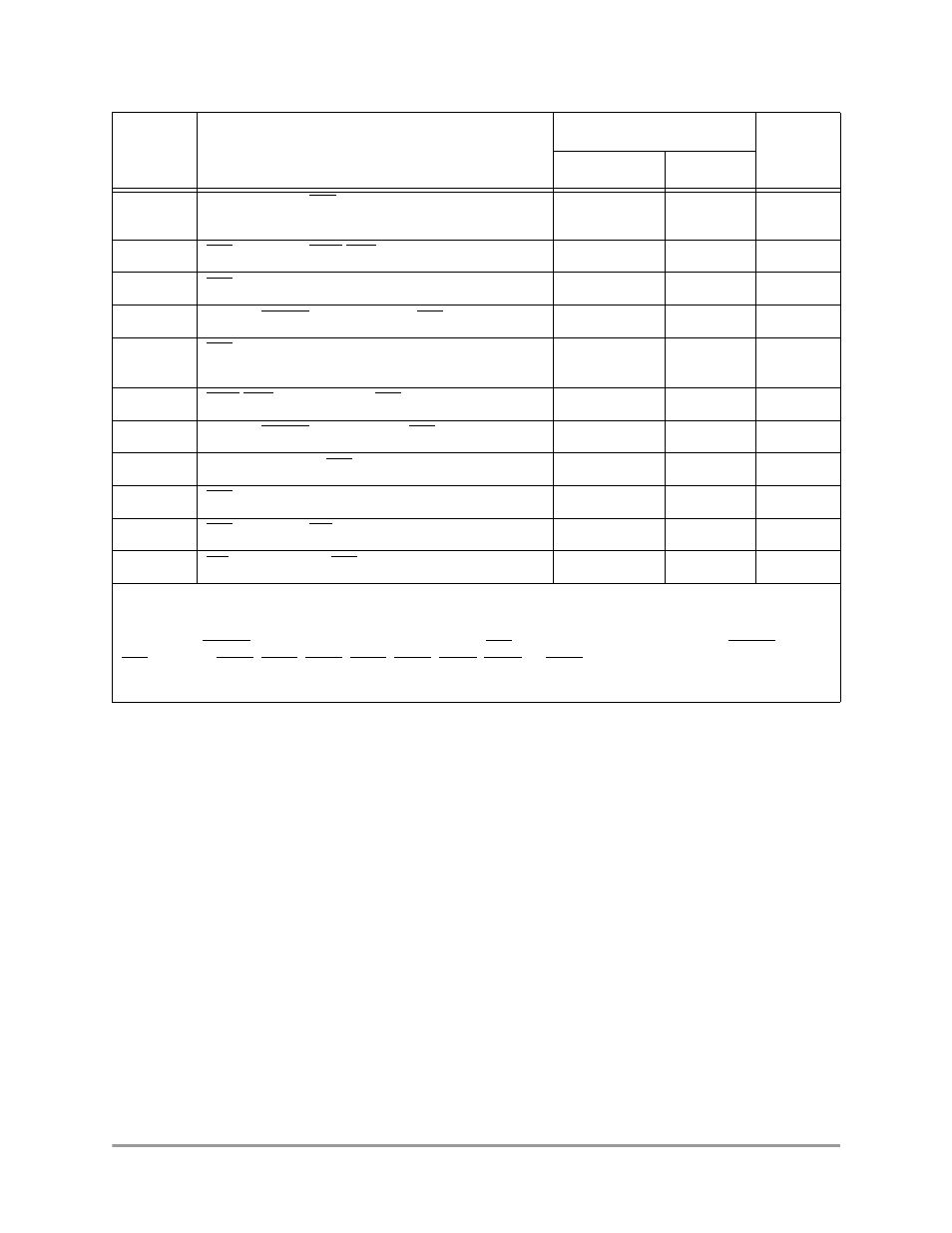
Figure 19-4 on page 19-7 shows the flash write cycle timing used by chip-select. The signal values and
units of measure for this figure are found in Table 19-6 on page 19-7. For detailed information about the
individual signals, see Chapter 6, “Chip-Select Logic.”
Table 19-5. Chip-Select Write Cycle Timing Parameters
Number
Characteristic
(3.0 ± 0.3) V
Unit
Minimum
Maximum
1
Address valid to CSx asserted
(bit ECDS = 0, bit ECDS = 1)
20, 20 - T/2
—
ns
2
CSx
asserted to UWE/LWE asserted
0
4
ns
3
CSx
asserted to data-out valid
—
30
ns
4
External DTACK
input setup from CSx
asserted
—
20 + nT
ns
5
CSx
pulse width
(bit ECDS = 0, bit ECDS = 1)
60 + nT,
(60 + T/2) + nT
—
ns
6
UWE/LWE negated before CSx
is negated
10
20
ns
7
External DTACK
input hold after CSx is negated
0
—
ns
8
Data-out hold after CSx
is negated
8
—
ns
9
CSx
negated to data-out in Hi-Z
—
18
ns
10
CSx
asserted to WE asserted (16-bit SRAM)
0
4
ns
11
WE negated before CSx
is negated (16-bit SRAM)
10
20
ns
Note:
n is the number of wait-states in the current memory access cycle.
T is the system clock period.
The external DTACK input requirement is eliminated when CSx is programmed to use the internal DTACK.
CSx stands for CSA0, CSA1, CSB0, CSB1, CSC0, CSC1, CSD0, or CSD1.
A value in parentheses is used when early detection is turned on.