28 spi 1 master using data_ready level trigger, 29 spi 1 master “don’t care” data_ready, 30 spi 1 slave fifo advanced by bit count – Motorola MC68VZ328 User Manual
Page 349: Spi 1 master using data_ready level trigger -33, Spi 1 master “don’t care” data_ready -33, Spi 1 slave fifo advanced by bit count -33, Figure 19-29 spi 1 master using
AC Electrical Characteristics
Electrical Characteristics
19-33
19.3.28
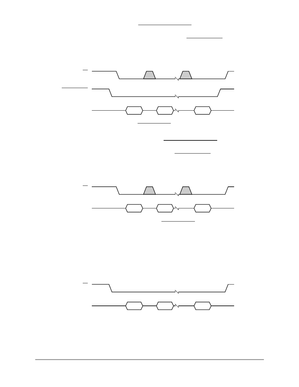
SPI 1 Master Using DATA_READY Level Trigger
Figure 19-29 shows the timing diagram for the SPI 1 master using the DATA_READY level trigger. The
signal values and units of measure for Figure 19-27 through Figure 19-32 are found in Table 19-17 on
page 19-34. Detailed information about the operation of individual signals can be found in Chapter 13,
“Serial Peripheral Interface 1 and 2.”
Figure 19-29. SPI 1 Master Using DATA_READY Level Trigger Timing Diagram
19.3.29
SPI 1 Master “Don’t Care” DATA_READY
Figure 19-30 shows the timing diagram for the SPI 1 master with DATA_READY “don’t care.” The signal
values and units of measure for Figure 19-27 through Figure 19-32 are found in Table 19-17 on
page 19-34. Detailed information about the operation of individual signals can be found in Chapter 13,
“Serial Peripheral Interface 1 and 2.”
Figure 19-30. SPI 1 Master “Don’t Care” DATA_READY Timing Diagram
19.3.30
SPI 1 Slave FIFO Advanced by Bit Count
Figure 19-31 shows the timing diagram for the SPI 1 slave FIFO advanced by bit count. The signal values
and units of measure for Figure 19-27 through Figure 19-32 are found in Table 19-17 on page 19-34.
Detailed information about the operation of individual signals can be found in Chapter 13, “Serial
Peripheral Interface 1 and 2.”
Figure 19-31. SPI 1 Slave FIFO Advanced by Bit Count Timing Diagram
SS
(Output)
DATA_READY
(Input)
SCLK,
MOSI, MISO
SS
(Output)
SCLK,
MOSI, MISO
SS
(Input)
SCLK,
MOSI, MISO