3 pin layout of the ttl interface board, 4 pin layout of the htl interface board, 2 pin layout of the power supply socket on pwm 8 – HEIDENHAIN PWM 8 User Manual
Page 38
-
38
-
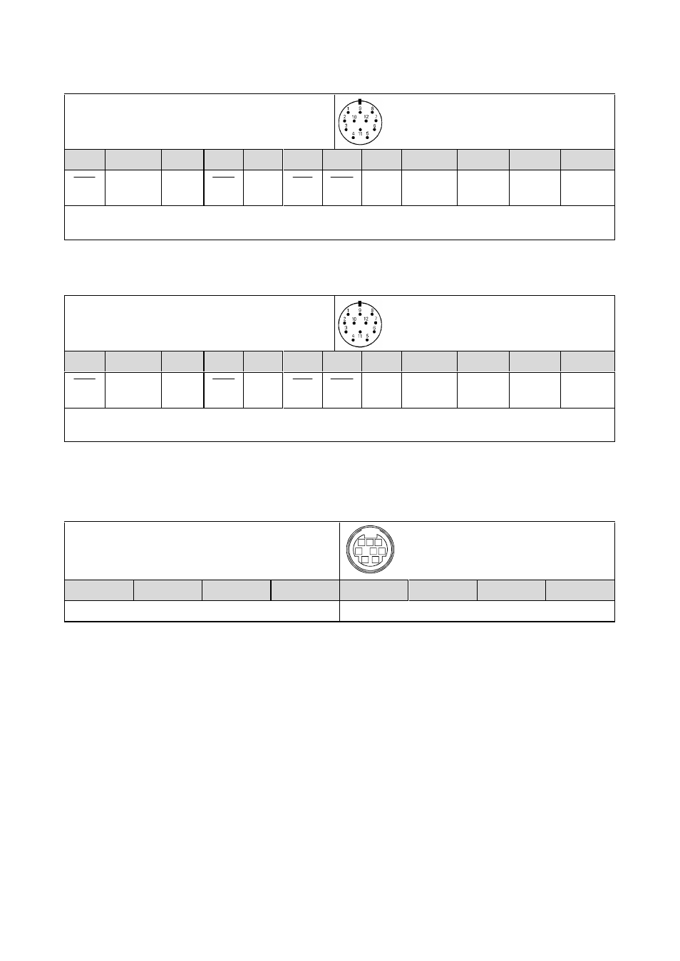
8.1.3 Pin Layout of the TTL Interface Board
12-pin HEIDENHAIN flange socket
at
IN
flange socket of the interface board
at
OUT
flange socket of the interface board
1
2
3
4
5
6
7
8
9
10
12
11
Ua2
+5 V
sensor
Ua0
Ua0
Ua1
Ua1
UaS
Ua2
chassis 0
V
UN
+5 V
UP
0 V
sensor
The sensor lines are connected to the corresponding supply lines
(exception: PWM 8 MODE: MEASURE U/I).
8.1.4 Pin Layout of the HTL Interface Board
12-pin HEIDENHAIN flange socket
at
IN
flange socket of the interface board
at
OUT
flange socket of the interface board
1
2
3
4
5
6
7
8
9
10
12
11
Ua2
10-30 V
sensor
Ua0
Ua0
Ua1
Ua1
UaS
Ua2
chassis 0
V
UN
10-30 V
UP
0 V
sensor
The sensor lines are connected to the corresponding supply lines
(exception: PWM 8 MODE: MEASURE U/I).
8.2 Pin Layout of the Power Supply Socket on PWM 8
8-pin power supply socket DC-IN
8
7 6
5
4
3
2
1
1
2
3
4
5
6
7
8
10-30V 0V