Kalypso classic video timing and delay – Grass Valley Kalypso Installation Planning Guide User Manual
Page 60
60
Kalypso Installation Planning Guide
Section 3 — Kalypso Classic Frame
Kalypso Classic Video Timing and Delay
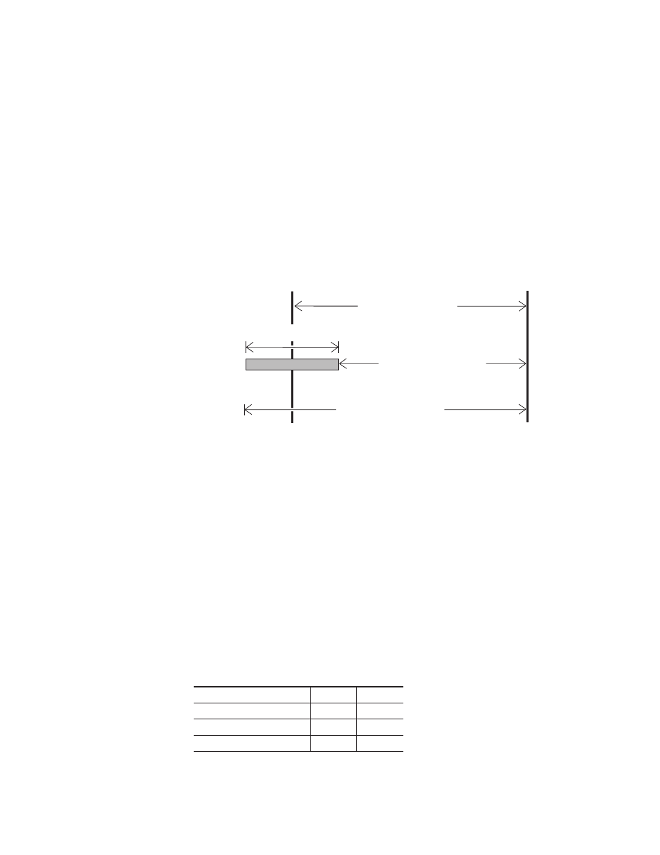
The total delay of a video input to the switcher output can vary according
to the relationship of the input to the switcher reference. The switcher will
automatically autotime inputs that fall within an autotiming window
(± B µs). Inputs must be within this range to be properly timed at the
output. The calculation of the actual video delay of a specific input is the
Nominal Switcher Delay minus the input time location within the
autotiming window (the time location value can be zero, positive, or nega-
tive). A timing diagram of the input autotiming window and various
switcher delay values is provided in
.
Figure 64. Switcher Timing Diagram
Note
For both 525 and 625 switcher operation, the approximate maximum
switcher delay is one line of video.
•
For inputs entering the switcher in zero time with the reference, the
total delay through the switcher is the Nominal Switcher Delay (A µs).
•
Inputs that reach the switcher at the latest point in the autotiming
window (+B µs) will have a total delay that equals the time required for
switcher processing. This value is the Minimum Switcher Delay (C µs).
•
Inputs that reach the switcher at the earliest point in the autotiming
window (-B µs) will have a total delay equal to the Nominal Switcher
Delay (A µs) plus the autotiming window range. This value is the
Maximum Switcher Delay value (D µs).
Delay values for a Kalypso system are given in
.
Table 15. Kalypso System Video Delay Values
Nominal Switcher Delay
A
53 µs
Serial Input Autotiming
B
+/- 10 µs
Minimum Switcher Delay
C
43 µs
Maximum Switcher Delay
D
63 µs
Nominal Output
Timing
Serial Input
Autotiming
Window
+/- B
µs
Nominal Reference
Timing
8096_03_05_r1
Nominal Switcher Delay
A
µs
Maximum Switcher Delay
D
µs
Minimum Switcher Delay
C
µs
- B
µs
+ B
µs
0
µs