Altera Stratix II EP2S180 DSP Development Board User Manual
Page 43
Altera Corporation
Core Version a.b.c variable
2–35
Stratix II EP2S180 DSP Development Board Reference Manual
Board Components & Interfaces
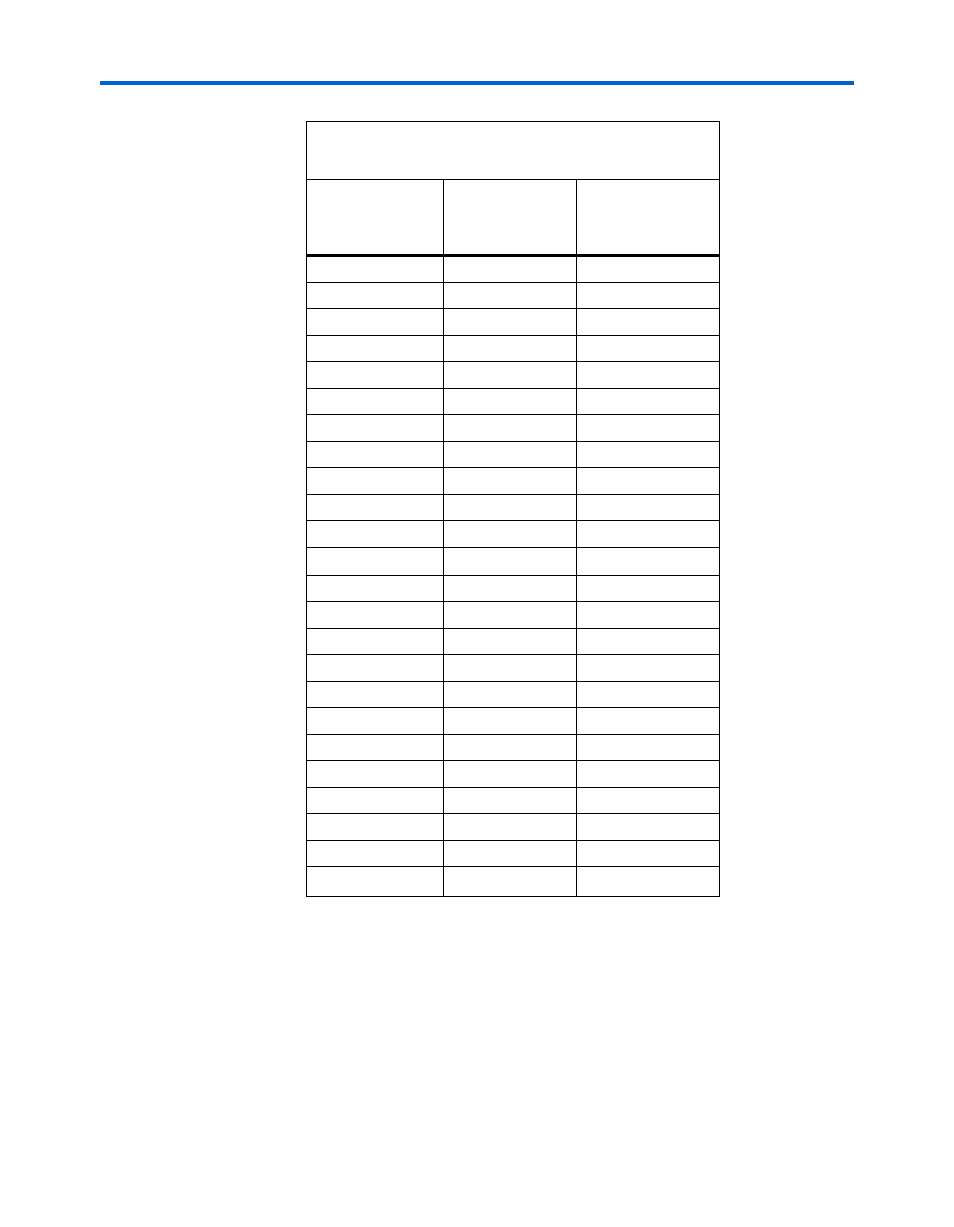
27
D11
AA2
28
D12
AA4
29
D13
Y5
30
D14
AB2
31
D15
AB4
32
CS1#
AC9
33
VS1#
AB10
34
IORD#
AC2
35
IOWR#
AC1
36
WE#
AC6
37
INTRQ
AC4
38
VCC
V
CC
(2)
39
CSEL#
AC8
40
VS2# AB9
41
RESET
AE12
42
WAIT#
AC3
43
INPACK#
AC7
44
REG#
AB7
45
DASP#
AE4
46
PDIAG#
AF2
47
DO8
V3
48
DO9
W2
49
D10
Y3
50
VSS
GND
(3)
Notes to
Table 2–28
:
(1)
All pin numbers represent I/O pins on the FPGA, unless
otherwise noted.
(2)
This FPGA I/O pin controls a power MOSFET that supplies
5V V
CC
to CON1.
(3)
This pin does not connect to the FPGA directly.
(4)
RESET is driven by the EPM7256AE configuration
controller device.
Table 2–28. CompactFlash (CON1) Pin Table (Part 2
of 2)
Pin on
CompactFlash
(CON1)
CompactFlash
Function (U60)
Connects to
(1)
- MAX 10 JTAG (15 pages)
- MAX 10 Power (21 pages)
- Unique Chip ID (12 pages)
- Remote Update IP Core (43 pages)
- Device-Specific Power Delivery Network (28 pages)
- Device-Specific Power Delivery Network (32 pages)
- Hybrid Memory Cube Controller (69 pages)
- ALTDQ_DQS IP (117 pages)
- MAX 10 Embedded Memory (71 pages)
- MAX 10 Embedded Multipliers (37 pages)
- MAX 10 Clocking and PLL (86 pages)
- MAX 10 FPGA (26 pages)
- MAX 10 FPGA (56 pages)
- USB-Blaster II (22 pages)
- GPIO (22 pages)
- LVDS SERDES (27 pages)
- User Flash Memory (33 pages)
- ALTDQ_DQS2 (100 pages)
- Avalon Tri-State Conduit Components (18 pages)
- Cyclone V Avalon-MM (166 pages)
- Cyclone III FPGA Starter Kit (36 pages)
- Cyclone V Avalon-ST (248 pages)
- Stratix V Avalon-ST (286 pages)
- Stratix V Avalon-ST (293 pages)
- DDR3 SDRAM High-Performance Controller and ALTMEMPHY IP (10 pages)
- Arria 10 Avalon-ST (275 pages)
- Avalon Verification IP Suite (224 pages)
- Avalon Verification IP Suite (178 pages)
- FFT MegaCore Function (50 pages)
- DDR2 SDRAM High-Performance Controllers and ALTMEMPHY IP (140 pages)
- Floating-Point (157 pages)
- Integer Arithmetic IP (157 pages)
- Embedded Peripherals IP (336 pages)
- JESD204B IP (158 pages)
- Low Latency Ethernet 10G MAC (109 pages)
- LVDS SERDES Transmitter / Receiver (72 pages)
- Nios II Embedded Evaluation Kit Cyclone III Edition (3 pages)
- Nios II Embedded Evaluation Kit Cyclone III Edition (80 pages)
- IP Compiler for PCI Express (372 pages)
- Parallel Flash Loader IP (57 pages)
- Nios II C2H Compiler (138 pages)
- RAM-Based Shift Register (26 pages)
- RAM Initializer (36 pages)
- Phase-Locked Loop Reconfiguration IP Core (51 pages)
- DCFIFO (28 pages)