Altera Stratix II EP2S180 DSP Development Board User Manual
Page 25
Altera Corporation
Core Version a.b.c variable
2–17
Stratix II EP2S180 DSP Development Board Reference Manual
Board Components & Interfaces
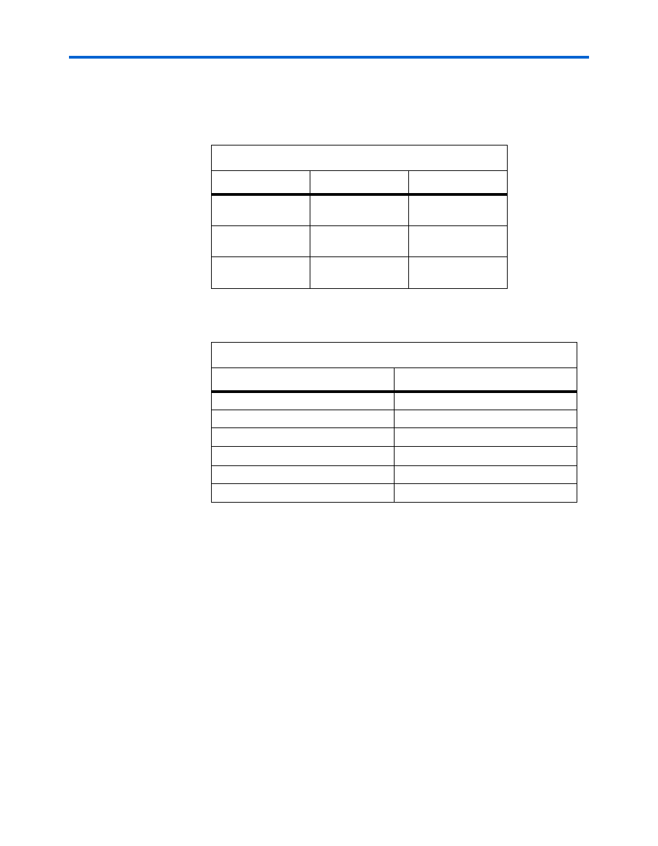
to select the clock for ADC B.
Table 2–10
explains how to select these three
clock signals. The selected clock will pass through a differential LVPECL
buffer before arriving at the clock input to both A/D converters
Table 2–11
lists reference information for the A/D converters.
Table 2–10. A/D Clock Source Settings
J3, J4 Setting
Clock Source
Signal Name
Pins 1 and 2
Stratix II PLL
circuitry
adc_PLLCLK1,
adc_PLLCLK2
Pins 3 and 4
OSC or External
input clock positive
adc_CLK_IN1,
adc_CLK_IN2
Pins 5 and 6
OSC or External
input clock negative
adc_CLK_IN1_n,
adc_CLK_IN2_n
Table 2–11. A/D Converter Reference
Item
Description
Board reference
U1, U2
Part number
AD9433BSQ
Device description
12-bit, 125-MSPS A/D converter
Voltage
3.3-V digital V
DD
, 5.0-V analog V
DD
Manufacturer
Analog Devices
Manufacturer web site
www.analog.com
- MAX 10 JTAG (15 pages)
- MAX 10 Power (21 pages)
- Unique Chip ID (12 pages)
- Remote Update IP Core (43 pages)
- Device-Specific Power Delivery Network (28 pages)
- Device-Specific Power Delivery Network (32 pages)
- Hybrid Memory Cube Controller (69 pages)
- ALTDQ_DQS IP (117 pages)
- MAX 10 Embedded Memory (71 pages)
- MAX 10 Embedded Multipliers (37 pages)
- MAX 10 Clocking and PLL (86 pages)
- MAX 10 FPGA (26 pages)
- MAX 10 FPGA (56 pages)
- USB-Blaster II (22 pages)
- GPIO (22 pages)
- LVDS SERDES (27 pages)
- User Flash Memory (33 pages)
- ALTDQ_DQS2 (100 pages)
- Avalon Tri-State Conduit Components (18 pages)
- Cyclone V Avalon-MM (166 pages)
- Cyclone III FPGA Starter Kit (36 pages)
- Cyclone V Avalon-ST (248 pages)
- Stratix V Avalon-ST (286 pages)
- Stratix V Avalon-ST (293 pages)
- DDR3 SDRAM High-Performance Controller and ALTMEMPHY IP (10 pages)
- Arria 10 Avalon-ST (275 pages)
- Avalon Verification IP Suite (224 pages)
- Avalon Verification IP Suite (178 pages)
- FFT MegaCore Function (50 pages)
- DDR2 SDRAM High-Performance Controllers and ALTMEMPHY IP (140 pages)
- Floating-Point (157 pages)
- Integer Arithmetic IP (157 pages)
- Embedded Peripherals IP (336 pages)
- JESD204B IP (158 pages)
- Low Latency Ethernet 10G MAC (109 pages)
- LVDS SERDES Transmitter / Receiver (72 pages)
- Nios II Embedded Evaluation Kit Cyclone III Edition (3 pages)
- Nios II Embedded Evaluation Kit Cyclone III Edition (80 pages)
- IP Compiler for PCI Express (372 pages)
- Parallel Flash Loader IP (57 pages)
- Nios II C2H Compiler (138 pages)
- RAM-Based Shift Register (26 pages)
- RAM Initializer (36 pages)
- Phase-Locked Loop Reconfiguration IP Core (51 pages)
- DCFIFO (28 pages)