Functional description, Power, Functional description –8 – Altera Stratix II EP2S180 DSP Development Board User Manual
Page 16: 2 v), v, 3 v), and v, Leds, Switches, Crystal oscillator
2–8
Core Version a.b.c variable
Altera Corporation
Stratix II EP2S180 DSP Development Board Reference Manual
Functional Description
Functional
Description
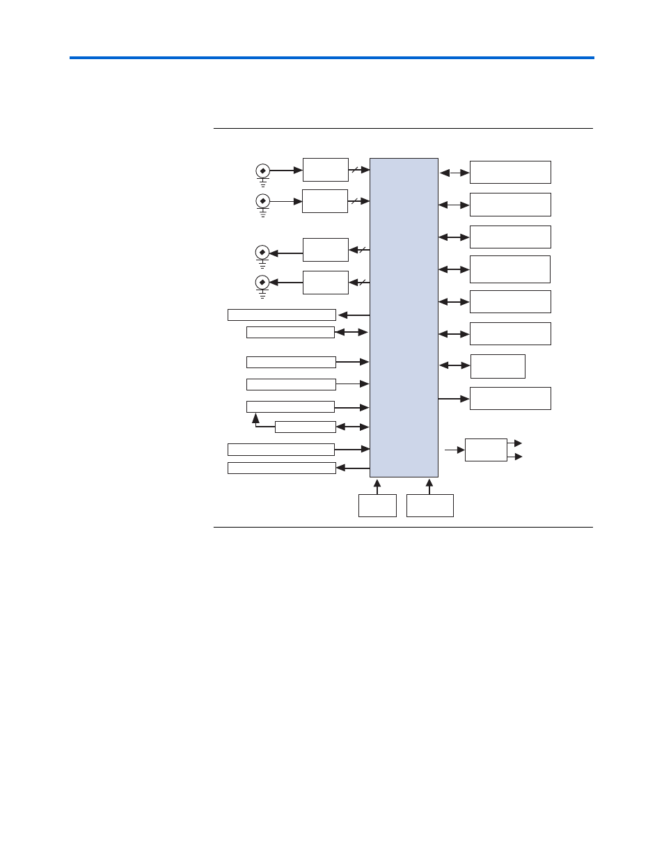
This section describes the elements of the Stratix II EP2S180 DSP
development board.
Figure 2–2
shows a block diagram of the board.
Figure 2–2. Stratix II EP2S180 Development Board Block Diagram
Power
The 16-layer development board has 10 signal layers and 6 ground/VCC
planes. The board is powered from a single, well regulated 16-V supply.
Regulators on the board are used to develop the V
CCINT
(1.2 V), V
CCIO
(3.3 V), and V
CC5
(5.0 V) voltages. The board includes a Power-on LED
that indicates the presence of V
CCIO
.
The following board elements are powered by the 3.3 V supply:
■
LEDs
■
Switches
■
Crystal oscillator
SMA External Clock Input
SMA External Clock Output
256K
× 36 SRAM
Mictor Connector
256K
× 36 SRAM
14
D/A
Converter
14
D/A
Converter
Stratix II
EP2S180
Device
JTAG Connector
Regulators
RS-232
5.0 V
Vccint (1.5 V)
Vccio (3.3-V)
80-MHz Oscillator
Prototyping Area
LEDs
Pushbutton
Switches
DIP
Switches
TI-EVM Connector
32 Mbit Flash
Analog Devices
A/D Converters
Connector
Dual Seven-Segment Display
12
A/D
Converter
12
A/D
Converter
0.1-inch Digital
I/O Headers
Configuration Controller