Clocks & clock distribution – Altera Stratix II EP2S180 DSP Development Board User Manual
Page 17
Altera Corporation
Core Version a.b.c variable
2–9
Stratix II EP2S180 DSP Development Board Reference Manual
Board Components & Interfaces
Table 2–3
lists the reference information for the 16-V power supply,
which connects from the wall socket to the DSP development board.
Clocks & Clock Distribution
lists the clocks and their signal distribution throughout the
board.
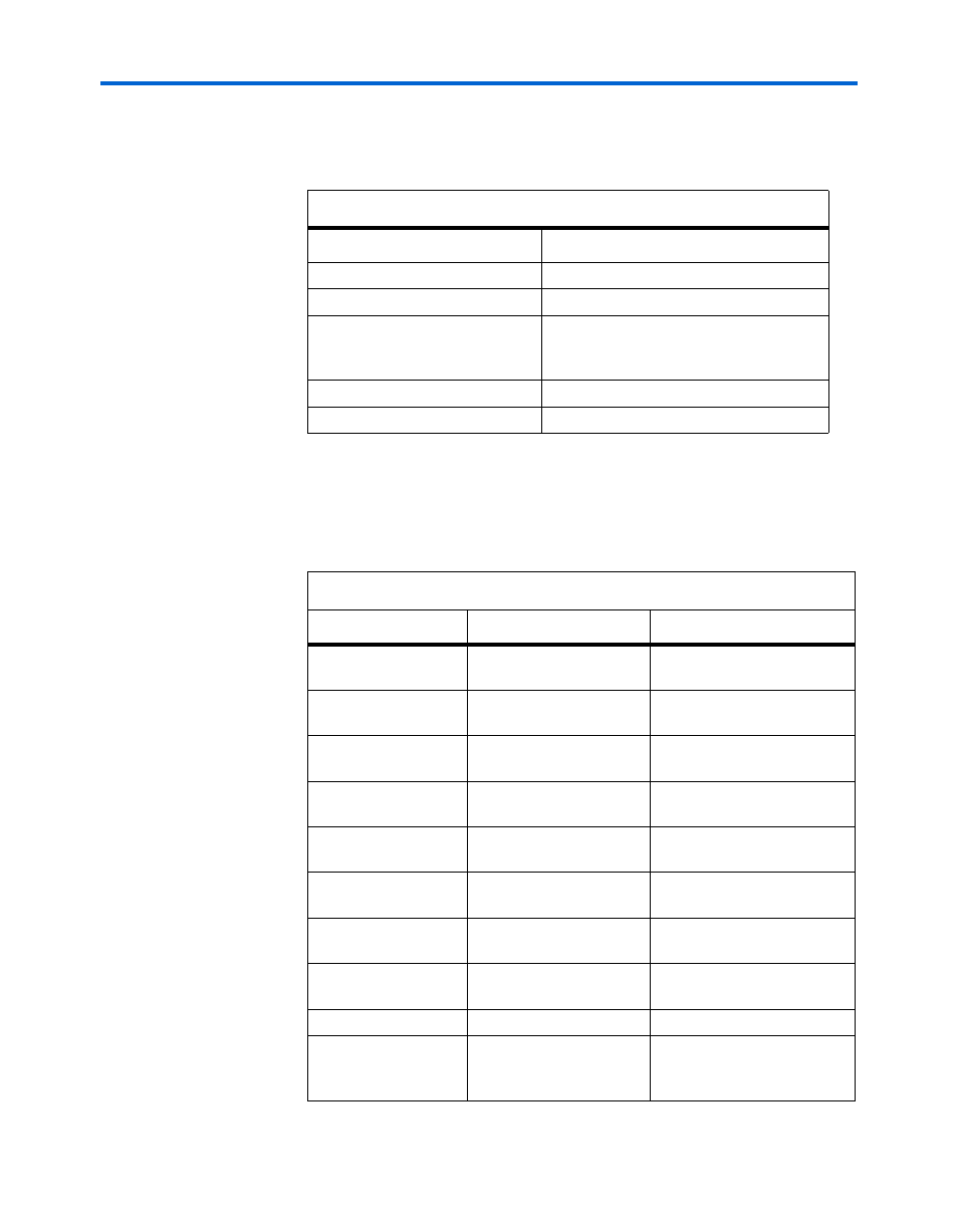
Table 2–3. Power Supply Specifications
Item
Description
Board reference
N/A (power supply adapter)
Part number
TR9KT3750LCP-Y
Device description
Switching power supply,
Input: 100-240 V, ~1.2 A max., 50-60
Hz Output: +16 V, 3.75 A, 60 W max.
Manufacturer
GlobTek Inc.
Manufacturer web site
www.globtek.com
Table 2–4. Clock Distribution Signals (Part 1 of 2)
Signal Name
Comes From
Goes To
dac_PLLCLK1
Stratix II device pin B15
(PLL5_OUT0p)
DAC A (U14 pin 28)
dac_PLLCLK1_n
Stratix II device pin C15
(PLL5_OUT0n)
DAC A (U14 pin 28)
dac_PLLCLK2
Stratix II device pin C16
(PLL5_OUT1p)
DAC B (U15 pin 28)
dac_PLLCLK2_n
Stratix II device pin D16
(PLL5_OUT1n)
DAC B (U15 pin 28)
sdram_CLK
Stratix II device pin AK16
(PLL6_OUT0p)
SDRAM (U39 U40 pins 68)
adc_PLLCLK1
Stratix II device pin B18
(PLL11_OUT0p)
ADC A (U1 pins 8, 7)
(1)
adc_PLLCLK2
Stratix II device pin
D18(PLL11_OUT0n)
ADC B (U2 pins 8, 7)
(1)
audio_CLK
Stratix II device pin
AL18(PLL12_OUT0p)
Audio CODEC (U5 pin 25)
pld_MICTORCLK
Stratix II device pin M25
Mictor Connector (J20 pin 5)
pld_CLKOUT
Stratix II device pin J14
PROTO1 (J25 pin 11) and
PROTO2 (J28 pin 11) via a
buffer (U7)