System management bus (smbus) watchdog timer, Table 3-14, Smbus reserved addresses – ADLINK ReadyBoard 910 User Manual
Page 41: Table 3-15, Smbus data interface pin signal descriptions (jp7), Table 3-16
Chapter 3
Hardware
ReadyBoard 910
Reference Manual
35
System Management Bus (SMBus)
The PCH contains both a host and slave SMBus ports; but the host cannot access the slave internally. The
slave port allows an external master access to the PCH through headers JP7 and JP8. The master is used to
communicate with the SODIMMs.
lists the slave device names and corresponding reserved
binary addresses on the SMBus.
lists the pin signals for the SMBus DATA header, which
provides 2 pins, 1 row, and 0.079" (2mm) pitch.
lists the pin signals for the SMBus CLOCK
header, which provides 2 pins, 1 row, and 0.079" (2mm) pitch.
Note: The shaded area denotes power or ground. The signals marked with * = Negative true logic.
Watchdog Timer
The Watchdog Timer (WDT) restarts the system if a mishap occurs. Possible problems include failure to
boot properly, the application software’s loss of control, unexpected conditions on the bus, or other hardware
or software malfunctions.
The WDT (Watchdog Timer) can be used both during the boot process and during normal system operation.
•
During the Boot process – If the operating system fails to boot in the time interval set in the BIOS, the
system will reset.
Enable the WDT in the Boot Settings of BIOS Setup. Set the WDT for a time-out interval in seconds,
between 1 and 255, in one second increments. Ensure you allow enough time for the operating system
(OS) to boot. The OS or application must tickle the WDT before the timer expires.
•
During System Operation – An application can set up the WDT hardware through a BIOS call, or by
accessing the hardware directly. Some ADLINK Board Support Packages provide an API interface to
the WDT. The application must tickle the WDT before the timer expires or the system will be reset. The
BIOS implements interrupt 15 function 0C3h to manipulate the WDT.
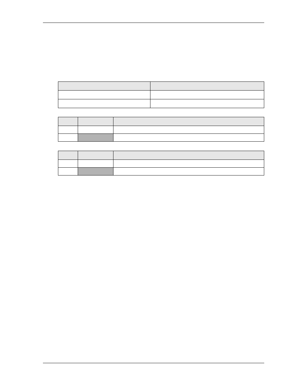
Table 3-14. SMBus Reserved Addresses
Component
Address (Hex)
SODIMM A
A0h
SODIMM B
A4h
Table 3-15. SMBus DATA Interface Pin Signal Descriptions (JP7)
Pin #
Signal
Description
1
SMBDATA
SMBus Data
2
+3.3V
+3.3V standby voltage
Table 3-16. SMBus CLOCK Interface Pin Signal Descriptions (JP8)
Pin #
Signal
Description
1
SMBCLOCK
SMBus Clock
2
GND
Ground