Figure 2-5, Header and connector pin sequence – ADLINK ReadyBoard 910 User Manual
Page 19
Chapter 2
Product Overview
ReadyBoard 910
Reference Manual
13
Figure 2-5. Header and Connector Pin Sequence
CN23 – DDR3
SODIMM1 (on bottom
side)
Bottom
204-pin, standard socket for non-ECC, unbuffered DDR3
SODIMM
FN1 – CPU Fan
Top
3-pin, 0.100" (2.54 mm) header, providing +12V, tach, and ground
signals to CPU fan
FN2 – System Fan
Top
3-pin, 0.100" (2.54mm) header, providing +12V, tach, and ground
signals to System fan
JP5 – Beeper/Buzzer
Top
2-pin, 0.079" (2mm) header for 5V buzzer or beeper output
JP6 – Power Button
Top
2-pin, 0.100" (2.54mm) header for external power button
JP7 – SMBus Data
Top
2-pin, 0.079" (2mm) header for SMBus data output
JP8 – SMBus Clock
Top
2-pin, 0.079" (2mm) header for SMBus clock output
LED – Power and SATA
Activity
Top
4-pin LED array with yellow diode indicating HDD activity and
green diode indicating power
SW1 – Clear CMOS
Top
Non-Operational (Use
“Oops! Jumper (BIOS Recovery)” on
to clear CMOS)
SW2 – System Reset
Top
4-pin, push-button switch for hard reset
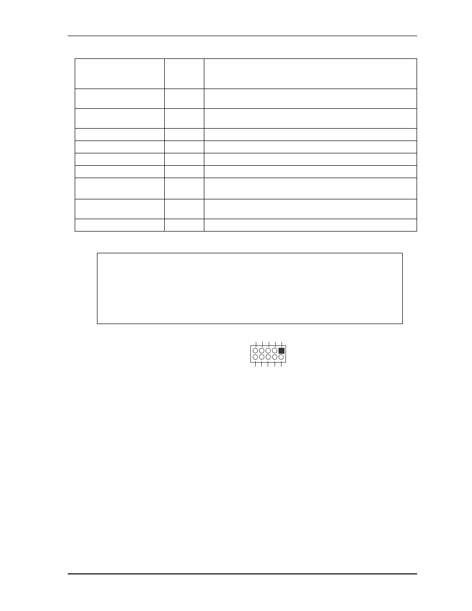
NOTE
The pinout tables in Chapter 3 of this manual identify pin sequence using the
following method: A 10-pin header with two rows of pins, using odd/even
numbering, where pin 2 is directly across from pin 1, is noted as 10-pin, 2 rows, odd/
even (1, 2).Alternately, a 10-pin connector using consecutive numbering, where pin 6
is directly across from pin 1, is noted in this way: 10-pin, 2 rows, consecutive (1, 6).
The second number in the parenthesis is always directly across from pin-1. See
.
Table 2-2. Header, Connector, and Socket Descriptions (Continued)
1
2
3
4
5
6
7
8
9
10
10-pin, two rows,
Odd/Even, (1, 2)
RB910_ConNum_a