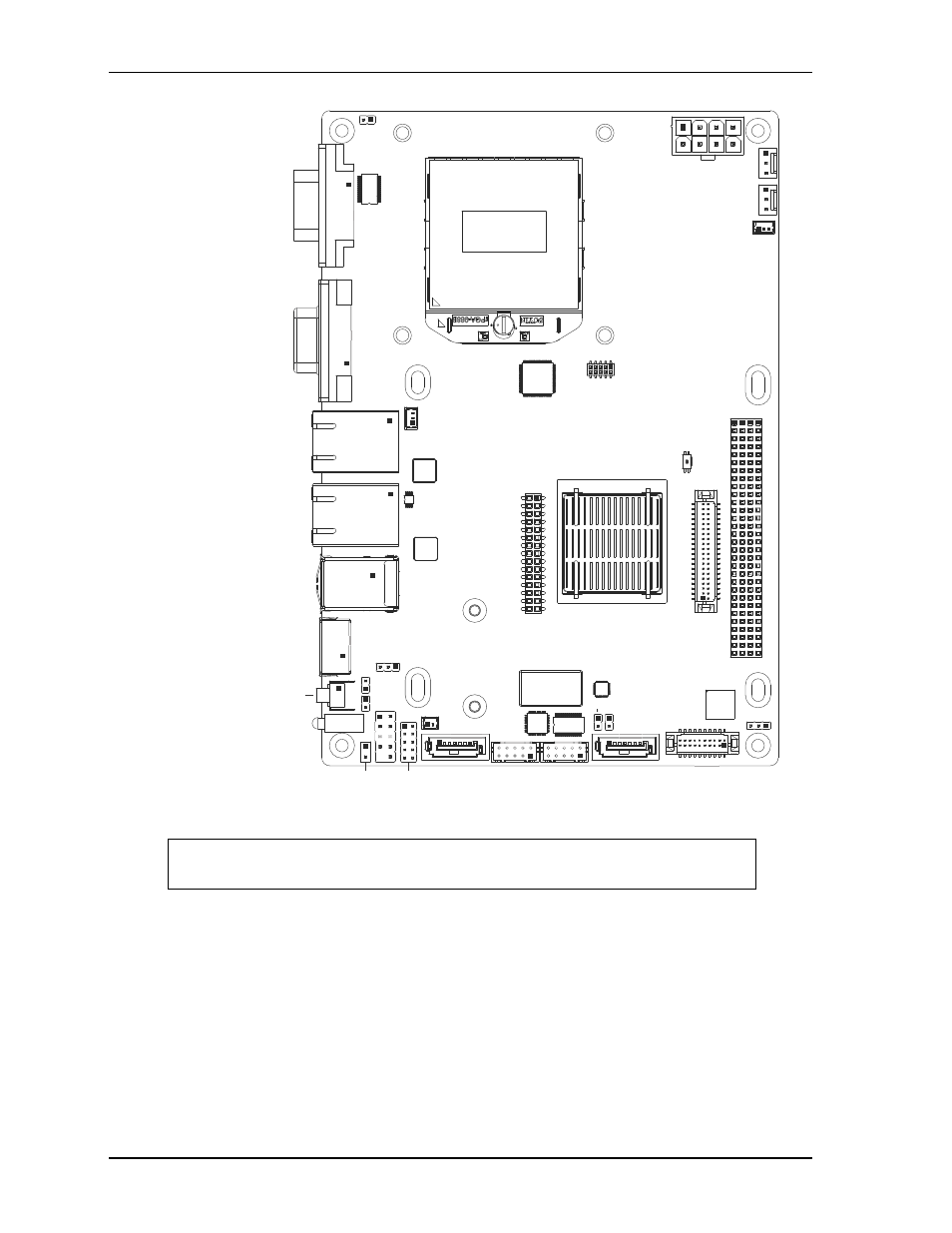
Figure 2-6, Header, connector, and socket locations – ADLINK ReadyBoard 910 User Manual
Page 20
Chapter 2
Product Overview
14
Reference Manual
ReadyBoard 910
Figure 2-6. Header, Connector, and Socket Locations
NOTE
Pin 1 is shown as a black pin (square or round) on all connectors and headers in
all illustrations.
CN18
CNX1
CN7
CN9
CN19
CN20
CN15
CN16
SW2
LED
JP6
JP4
JP3
JP2
JP7
JP8
JP5
JP1
CN14
CN13
CN11
CN10
CN8
CN12
CN6
CN5
CN2
SW1
CN1
FN2
FN1
CN3
CN4
RB910_T
op_Conn_c
Key:
CN1 - Power On
CNX1 - Digital Audio SPDF I/O
CN2 - PCI-104
CN3 - Power
CN4 - DVI
CN5 - LVDS
CN6 - SATA1
CN7 - LPC
CN8 - Serial 2 - COM1
CN9 - EXT
CN10 - Audio
CN11 - SATA2
CN12 - Battery
CN13 - GPIO
CN14 - USB 1-2
CN15 - USB Standard
CN16 - PS/2 Standard
CN17 - Serial 1 - COM0 (Standard DB9)
CN18 - VGA
CN19 - GLAN1 Standard RJ45
CN20 - GLAN2 Standard RJ45
CN21 - PCIe Mini Card (on bottom side)
CN22 - SODIMM2 (on bottom side)
CN22 - SODIMM1 (on bottom side)
FN1 - Fan (CPU)
FN2 - Fan (System)
JP5 - Beeper/Buzzer
JP6 - Power-On Button
JP7 - SMBus - Data
JP8 - SMBus - Clock
FN1 - Fan (CPU)
FN2 - Fan (System)
LED - Power and SATA Activity
SW1 - Non-Operational
SW2 - System Reset
Jumper Headers:
JP1 - See Jumper Table
(LVDS Panel Power Select)
JP2 - See Jumper Table
(RS-485 Termination Enable -
COM0)
JP3 - See Jumper Table
(RS-485 Termination Enable -
COM1)
JP4 - See Jumper Table
(Power Select S3/S5 Power On)
U30
CN17