Switches, Table 29: switches and their functions, Table 30: dip switches and their functions – Achronix Speedster22i HD1000 Development Kit User Guide User Manual
Page 66

66
UG034, July 1, 2014
Jumper
Implementation
Connected
Pins
Function
J46
Surface Mount
Resistor
1
Selects VDDL_REG
0.75V-1.2V
2
0.75V
3
1.0V
4
1.2V
J51
Surface Mount
Resistor
1
Selects VDD_BRAM_FB
0.75V-1.2V
2
0.75V
3
1.0V
4
1.2V
J53
Surface Mount
Resistor
None
1 & 2
Selects V3P3
2 & 3
Selects VBB_INLKN1
Note: ‘*’ denotes default setting.
Switches
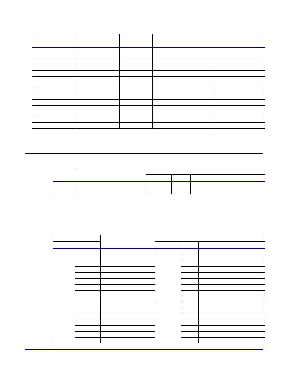
Table 29: Switches and their Functions
Switch
Function
Connection
Through
Pin
Comment
SW4
Generates RUN signals
U64
3
Drives ON_OFF_SW
S1
HD1000 reset*
U76
3
Drives FPGA_RESET1
* Usage of HD1000 reset requires a reset signal in the design to be routed to the IO
corresponding to the switch, which is pad2_clk_bank_sw = P17.
Table 30: DIP switches and their Functions
Switch
Function
Connection
No
Position
Through
Pin
Signal
SW13
1
PLL/Bypass mode
U102
40
E_VCCO_SEL_2
2
Output divider value
11
E_NA2_2
3
Output divider value
10
E_NA1_2
4
Output divider value
9
E_NA0_2
5
Output divider value
4
E_NB2_2
6
Output divider value
3
E_NB1_2
7
Output divider value
2
E_NB0_2
8
Clock divider input
1
E_M8_2
SW12
1
Clock divider input
48
E_M7_2
2
Clock divider input
47
E_M6_2
3
Clock divider input
46
E_M5_2
4
Clock divider input
45
E_M4_2
5
Clock divider input
44
E_M3_2
6
Clock divider input
43
E_M2_2
7
Clock divider input
42
E_M1_2
8
Clock divider input
41
E_M0_2
