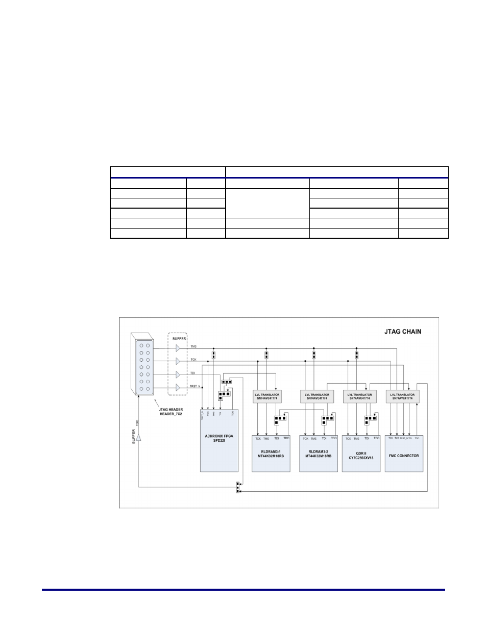
Jtag (j11), Figure 12: acx-brd-hd1000-100g jtag daisy chain – Achronix Speedster22i HD1000 Development Kit User Guide User Manual
Page 39

UG034, July 1, 2014
39
JTAG (J11)
You can use the JTAG interface for communicating with the board. This interface lets you
access the JTAG interface pins on the HD1000. In addition, information is transferred from
the board to the development PC. The header can be seen in Figure 2. You can use this
information for further debug, development or application actions. The signal pins for the 14-
pin are listed in Table 11.
Table 11: ACX-BRD-HD1000-100G JTAG Header (J11) Pins.
JTAG Header (J11)
Connection
Signal
Pin
Through
Signal Name
Pin
A_TRST_N
1
FMC Connector (J3)
FMC_TRST_N
D34
A_TMS
7
FMC _TMS
D33
A_TCK
9
FMC _TCK
D29
A_TDO
5
Jumper (J54)
A_TDO
1
A_TDI
3
Jumper (J19)
FPGA_TDI
2
The JTAG header pin A_TDI drives the FPGA_TDI pin TBD on the HD1000. This is daisy
chained using the TDO and TDI pins and jumpers to the RLDRAM3 devices (U31, U36), the
QDR2 device (U22) and the FMC connector (J3). The TDO signal from the FMC connector
goes back to the JTAG header (J11) to complete the daisy chain.
The daisy chain is shown in Figure 12.
J11
J12
J33
J40
J30
J19
J54
J32
J39
J27
J17
Figure 12: ACX-BRD-HD1000-100G JTAG Daisy Chain
Note: Figure 12 shows only the logical connection for application development. Relevant voltage
levels are driven on the board by additional circuitry.
